PVD Coating Methods: A 2025 Guide to Types and Selection
Introduction
Physical Vapor Deposition (PVD) is a cornerstone of modern manufacturing, but with multiple methods available, choosing the right one is critical. This guide doesn’t just list the PVD coating types—it provides a clear framework for comparing and selecting the ideal process based on your material, application, and budget.
Quick Navigation:
At a Glance: PVD Methods Comparison
Before diving into the details, this table provides a high-level overview to help you quickly narrow down your options.
| PVD Method | Best For | Key Advantage | Primary Limitation |
|---|---|---|---|
| Thermal Evaporation (Vacuum Evaporation) | Microelectronics, simple coatings | Cost-effective, simple process | Line-of-sight only, poorer uniformity |
| Sputtering Deposition | Electronics, solar panels, complex shapes | Excellent uniformity, wide material choice | Higher cost, more complex equipment |
| Ion Plating | Tools, automotive, medical (high adhesion) | Superior film density and adhesion | Higher operational cost and energy use |
| Cathodic Arc Deposition | Hard, wear-resistant tool coatings | Extremely dense and hard coatings | Can produce micro-droplets (defects) |
| Pulsed Laser Deposition | R&D, complex oxides, precision films | Stochiometric transfer, precise control | High cost, low throughput (R&D scale) |
| Electron Beam PVD | High-temperature coatings (aerospace) | High purity, high deposition rate | High e |
In-Depth Breakdown of PVD Coating Methods
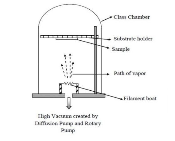
1. Thermal Evaporation (Vacuum Evaporation)
Vacuum evaporation is a foundational PVD technique where materials (referred to as the evaporating material) are heated in a vacuum to the point where they evaporate and then condense on a target substrate to form a thin film. This method is particularly effective with a wide range of materials, including metals, alloys, and organic compounds.
Process Description: In thermal evaporation, material from a resistive heating source (such as a tungsten filament or boat) is heated until it vaporizes. (Note: This distinguishes it from Electron Beam Physical Vapor Deposition, which uses a focused electron beam for heating.) The vapor travels through a vacuum chamber and deposits onto a cooler substrate, forming a uniform thin film. This process benefits from the low-pressure environment of the vacuum, which reduces the presence of contaminants and allows for a cleaner deposition.
Core Mechanism & Implications: This process relies purely on thermal energy to generate vapor. The evaporated atoms possess relatively low energy (typically around 0.1-0.5 eV) and travel in straight lines. This fundamental principle is the primary reason for its line-of-sight limitation and the challenges in uniformly coating complex geometries. However, the absence of plasma in the process typically results in very high-purity films.
Common Materials: Metals like aluminum, gold, and silver; dielectric materials; and organic semiconductors are commonly used. These materials can be effectively vaporized and deposited to create functional and decorative coatings.
Key Applications: Vacuum evaporation is integral in the fabrication of microelectronics, where it is used to form contacts and interconnects in devices. It is also used to deposit thin film resistors and dielectric layers in capacitors, demonstrating its versatility and precision in creating components with specific electrical properties.
Advantages Over Other Methods: Vacuum evaporation allows for high-purity films with excellent thickness control. It is a relatively simple and fast process that requires lower temperatures compared to other PVD methods, making it ideal for temperature-sensitive substrates. The equipment is generally less complex and more cost-effective, especially for small-scale productions or research applications.
From a technological evolution perspective, vacuum evaporation is the precursor of PVD technology. Modern mainstream techniques such as cathodic arc deposition and sputtering, while more advanced in terms of excitation sources and plasma control, all stem from the core principle of “vaporizing and depositing materials in a vacuum.”
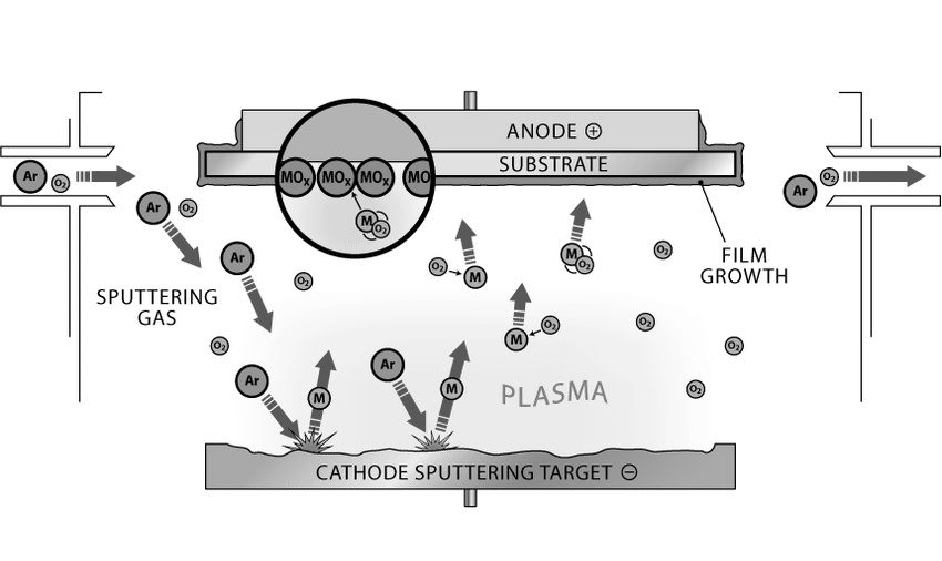
2. Sputtering Deposition
Sputtering deposition is a highly versatile PVD method that involves ejecting material from a target (or “sputter target“) through bombardment with energetic particles, usually ions, which then deposit onto a substrate to form a thin film. This method can be adapted to deposit a wide range of materials, including metals, ceramics, and plastics.
Process Description: In sputtering, a target material is placed in a vacuum chamber opposite the substrate. Ions generated in the plasma (often of an inert gas like Argon) within the chamber are accelerated towards the target with enough energy to dislodge atoms through momentum transfer. These atoms then travel through the vacuum and coat the substrate, forming a thin film. The process can be controlled to tailor film thickness and composition very precisely.
Core Mechanism & Implications: The sputtering process itself involves knocking atoms out of a solid target, which inherently allows for the deposition of a wide range of materials, including alloys and compounds with controlled composition. The ejected atoms have higher energy (1-10 eV) than in thermal evaporation, which improves adhesion and film density. The working pressure allows for more gas scattering, which reduces line-of-sight effects and enables more uniform coverage of complex geometries.
Varieties of Sputtering:
- Magnetron Sputtering: Utilizes magnetic fields to confine plasma close to the target surface, enhancing the efficiency of the ion bombardment and allowing for faster deposition rates.
- RF Sputtering (Radio Frequency Sputtering): Effective for insulating materials by using alternating current, thus avoiding charge build-up on the target.
- DC Sputtering (Direct Current Sputtering): Suitable for conductive materials, providing a steady ion stream.
- Ion-Beam Sputtering: Employs an ion beam directed at the target, allowing for more precise control over the deposition.
- Reactive Sputtering: Involves a reactive gas in the sputtering process, which forms a compound with the target material upon deposition.
Applications: Sputtering is commonly used to apply reflective coatings on glass, produce thin films for solar cells, and fabricate layers on semiconductor wafers. Its ability to coat complex shapes and features makes it invaluable in manufacturing electronics and display panels.
Benefits: This technique offers excellent control over film composition and thickness, making it possible to achieve specific electrical, optical, and mechanical properties. Sputtering can also cover large areas uniformly and is scalable from small research samples to large industrial components.
3. Ion Plating
Ion plating is a sophisticated PVD technique that enhances the adhesion and quality of thin films through the use of ionized vapor particles, which are accelerated towards the substrate under an electric field. This method is renowned for producing highly durable and adherent coatings, making it ideal for both functional and decorative applications.
Process Description: Ion plating involves evaporating the coating material, typically metals or alloys, in a vacuum chamber and then ionizing these vaporized particles using a plasma source. An electric field accelerates these ions towards the substrate, where they condense to form a thin film. This ion bombardment not only deposits the material but also increases the density and adhesion of the film through a process called “ion etching” that occurs simultaneously.
Core Mechanism & Implications: The key differentiator is the continuous low-energy ion bombardment of the substrate and the growing film. This bombardment performs several critical functions: it sputter-cleans the surface before deposition, provides additional energy for deposited atoms to migrate and form a dense structure (ion-assisted densification), and can even implant ions into the substrate, leading to exceptionally strong adhesion.
Common Materials: Materials frequently used in ion plating include titanium nitride (TiN), chromium, gold, and copper, each chosen for specific properties such as hardness, wear resistance, or aesthetic appeal.
Applications: Due to its strong film adhesion and versatility, ion plating is used extensively in the tool industry to extend the life of cutting and forming tools. It is also prevalent in the automotive sector for decorative trims and functional coatings that require enhanced durability. Additionally, the medical industry utilizes ion plating for surgical instruments and implants to improve biocompatibility and resistance to wear.
Advantages Over Other Methods: The ion bombardment mechanism makes ion plating capable of producing superior film density and strong adhesion, which can significantly improve wear and corrosion resistance when optimized. The method also allows for the coating of complex geometries and fine details, making it suitable for intricate designs and applications where precision is crucial.
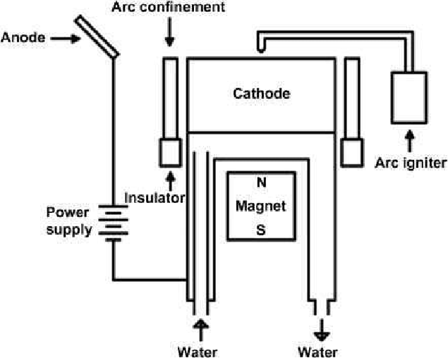
4. Cathodic Arc Deposition
Cathodic arc deposition, often referred to as arc PVD, is a method characterized by its ability to evaporate target materials through the use of an electric arc. This method excels in producing highly ionized vapor, which results in coatings that are extremely dense and adherent.
Process Description:The process involves striking a high-current, low-voltage electric arc directly onto a cathode target. The intense local heating instantaneously vaporizes and fully ionizes the material, creating a dense plasma plume. This plasma is then condensed onto the substrate to form a coating. The high degree of ionization (ranging from 30% to 100%) enhances the film’s mechanical properties and adhesion to the substrate.
Core Mechanism & Implications: The cathodic arc is characterized by an extremely high degree of ionization (often near 100%) and high ion energy (10-100 eV). When combined with a substrate bias, these highly energetic ions bombard the surface, resulting in extremely dense and hard coatings with compressive stress. However, the violent nature of the arc can also eject microscopic droplets of molten target material (“macros”), which can become defects in the film if not properly filtered.
Common Materials: Commonly used materials in cathodic arc deposition include titanium, chromium, and zirconium, which are ideal for creating hard, wear-resistant coatings.
Applications: Cathodic arc deposition is predominantly used for tool coatings in industries requiring high durability and resistance to wear, such as cutting tools and dies. It is also used for decorative coatings in the automotive and architectural sectors due to the excellent finish and color consistency it provides.
Advantages Over Other Methods: The high ionization and ion energy promote the formation of uniform and dense coatings, which typically exhibit exceptional hardness and wear resistance.
It also allows for better control over the chemical composition and microstructure of the coatings, leading to superior performance characteristics.
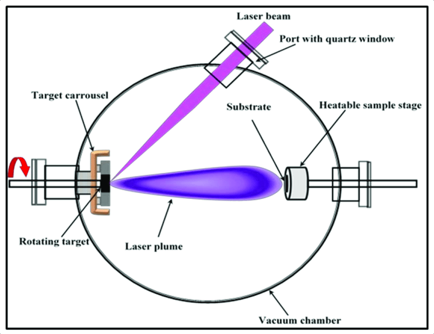
5. Pulsed Laser Deposition
Pulsed Laser Deposition (PLD) is a versatile PVD method that uses high-power laser pulses to vaporize material from a target, which then deposits on a substrate to form a thin film. This method is particularly favored for its ability to deposit a wide range of materials with precise control over the film’s composition and thickness.
Process Description: In PLD, a laser beam is directed at the target material in a vacuum chamber. The intense energy of the laser pulse vaporizes the surface of the target into a plasma plume, which then deposits on the substrate. The process allows for the deposition of materials with complex stoichiometries and high melting points.
Common Materials: PLD can be used with materials that are challenging to deposit by other methods, including high-temperature superconductors, complex oxides, and thin films for photovoltaics.
Applications: Due to its precise control over material deposition, PLD is extensively used in the electronics industry for developing advanced thin films in semiconductors and solar cells. It is also used in research environments for developing new material layers with unique properties.
Advantages Over Other Methods: PLD stands out for its ability to maintain the exact composition of the target material in the deposited film, which is crucial for functional materials in electronic and optical applications. The method also allows for rapid prototyping of multi-layer and multi-material structures, providing flexibility in research and development settings.
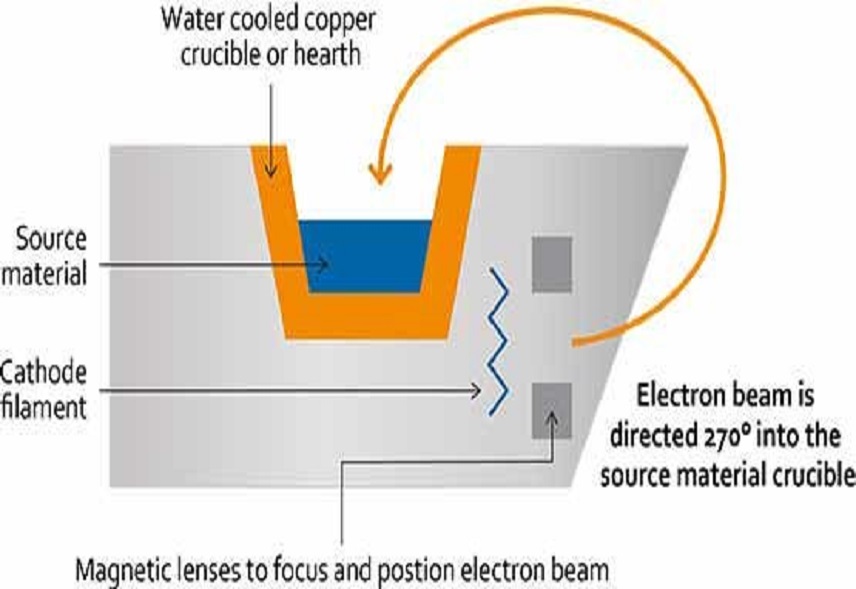
6. Electron Beam Physical Vapor Deposition
Electron Beam Physical Vapor Deposition (EBPVD) is a specialized PVD technique that uses an electron beam to heat and vaporize the target material in a vacuum, resulting in high-quality, pure thin films. This method is particularly effective for materials with high melting points and for applications requiring precise control over film properties.
Process Description: In EBPVD, an intense beam of electrons is focused on the target material, causing it to heat and eventually vaporize. The vaporized material then travels across the vacuum chamber and condenses on the substrate, forming a thin film. The process is conducted under high vacuum conditions, which minimizes contamination and allows for the deposition of very pure materials.
Common Materials: High-melting-point metals such as tungsten, molybdenum, and compounds like titanium nitrides are commonly used. These materials benefit from the high energy input of the electron beam, which can efficiently vaporize them despite their high melting temperatures.
Applications: EBPVD is widely used in the aerospace industry for coating turbine blades with thermal barrier coatings to enhance their durability and performance at high temperatures. It is also used in the semiconductor industry for depositing films with high electrical conductivity and in optical applications for anti-reflective coatings.
Advantages Over Other Methods: EBPVD offers several advantages, including high deposition rates and the ability to deposit extremely pure and dense films. It is particularly well-suited for applications requiring films with precise thickness and uniformity over large areas.
How to Choose the Right PVD Method
Use this flowchart to guide your decision-making process:
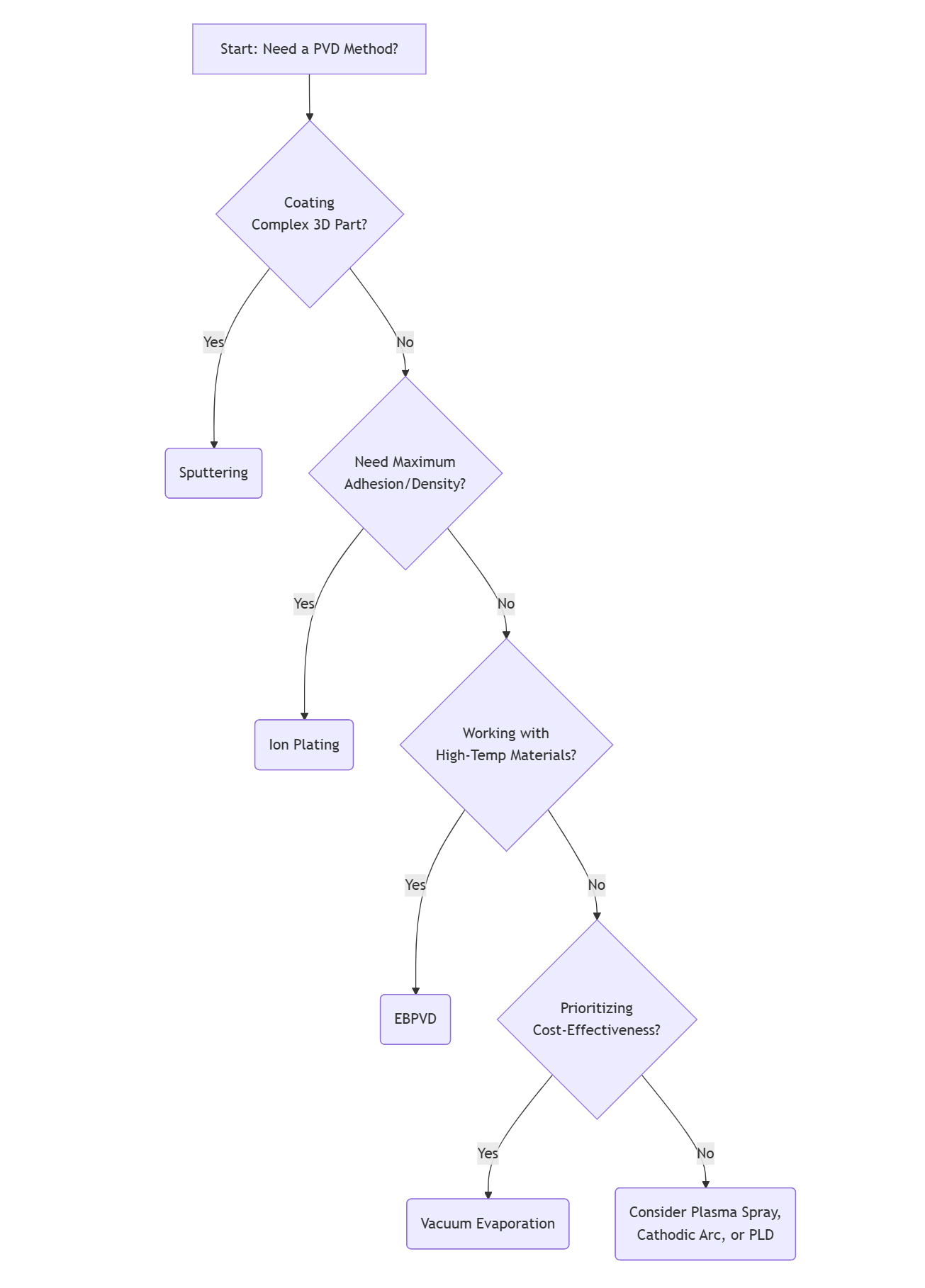
Key Decision Factors:
- Substrate Geometry: Complex shapes require non-line-of-sight methods like Sputtering.
- Film Properties: For maximum hardness and adhesion, consider Ion Plating or Cathodic Arc.
- Material: High-temperature materials often necessitate EBPVD.
- Budget & Scale: Cost-sensitive or R&D projects may favor Vacuum Evaporation.
- Throughput: For coating large areas quickly, Plasma Spray is unmatched.
Conclusion
From the simplicity of Vacuum Evaporation to the precision of Pulsed Laser Deposition, the optimal PVD method hinges on a balance of technical requirements and economic considerations.
Global PVD Materials Supply: Stanford Advanced Materials (SAM) is a global supplier of high-purity PVD coating materials, including sputtering targets and evaporation materials for a wide range of applications, supporting the industry’s evolving needs.
By understanding the strengths and trade-offs of each method outlined in this guide, engineers and designers can make informed decisions to optimize product performance, durability, and cost-effectiveness.


