An Overview of Electron Beam Evaporation
Electron Beam Evaporation – Definition
Electron beam evaporation, or E-beam evaporation, is a type of physical vapor deposition (PVD) technique, which directly heats the evaporation material (usually pellets) by using an electron beam under vacuum, and transports the vaporized material to the substrate to form a film.
Electron Beam Evaporation – Working Processes
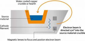
Electron beam evaporation is based on the evaporating of tungsten filaments. A current about 5 to 10 kV is sent through a tungsten filament (located outside the deposition area to avoid contamination) and heats it to the point where thermionic emission of electrons takes place. The electrons are focused and directed toward the evaporation materials (placed in a crucible) using permanent magnets or electromagnets. During the process when the electron beam hits the surface of the evaporation pellets, its kinetic energy is transformed to heat, and high energy (more than several million watts per square inch) is released. Thus, the hearth which holds the evaporating materials must be water-cooled to avoid melting.
Electron Beam Evaporation – Pros and Cons
Electron beam evaporation can evaporate high melting point materials, which is more efficient than general resistance heating and evaporation. Electron-beam evaporation can be widely used for optical coatings such as high purity film and conductive glass. It also has potential industrial applications for wear-resistant and thermal barrier coatings in aerospace industries, hard coatings for cutting and tool industries.
However, e-beam evaporation cannot be used to coat the inner surface of complex geometries. Besides, the filament degradation in the electron gun may result in a non-uniform evaporating rate.
Further Reading: Electron Beam Evaporation VS Thermal Evaporation
Electron Beam Evaporation – Applications
Because of its high deposition rate and high material utilization efficiency, e-beam evaporation is widely used in various applications. For example, the high-performance aerospace and automotive industries, which have high requirements for high temperature and wear resistance of materials; durable tool hard coatings; and chemical barriers and coatings to protect surfaces in corrosive environments. Electron beam evaporation is also used in optical films, including laser optics, solar panels, glasses, and architectural glass to give them the required conductive, reflective, and transmissive properties.
Electron Beam Evaporation V.S. Thermal Evaporation
The biggest difference between electron beam evaporation and thermal evaporation is: electron beam evaporation bombards an object with a beam of electrons which causes high energy for doing the evaporation, and thermal evaporation finishes the process by heating. Compared to thermal evaporation, e-beam evaporation gives high energy; but it will be difficult to control the thickness of the film in the order of 5 nm. In this case, a good thermal evaporator with a thickness monitor will be more suitable.
Electron beam evaporation has many advantages over thermal evaporation.
1) Electron beam evaporation can heat materials to a higher temperature than thermal evaporation. This allows very high deposition rates and evaporation of high-temperature materials and refractory metals such as tungsten, tantalum or graphite.
2) E-beam evaporation can deposit thinner films with higher purity. The water cooling of the crucible strictly limits the electron beam heating to the area occupied only by the source material, thereby eliminating any unnecessary contamination from adjacent components.
3) E-beam evaporation sources come in various sizes and configurations, including single or multiple cavities.
Stanford Advanced Materials (SAM) Corporation is a global evaporation material supplier. Please visit https://www.sputtertargets.net/ for more information.


