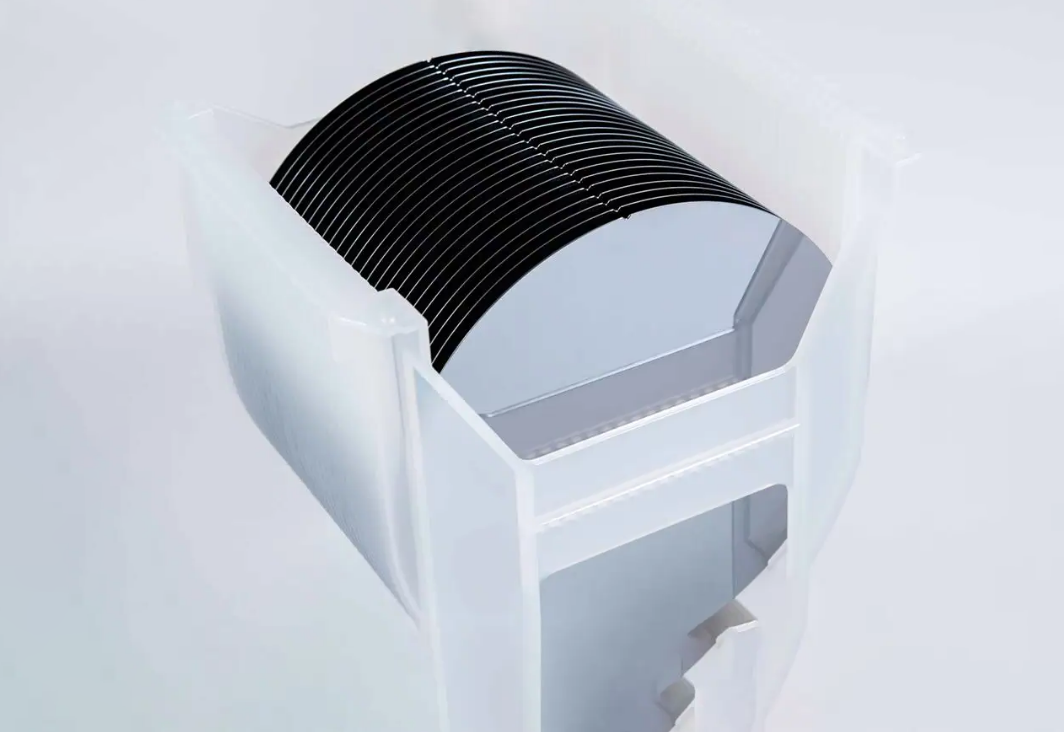
I. Introduction Silicon-on-insulator (SOI) technology represents a pivotal advancement in semiconductor manufacturing, offering enhanced performance and efficiency over traditional bulk silicon approaches. By integrating a thin silicon layer atop an insulating substrate, SOI facilitates superior electrical isolation and reduced parasitic capacitance, which is critical for high-performance electronic devices. SOI involves layering a silicon wafer on...Continue Reading
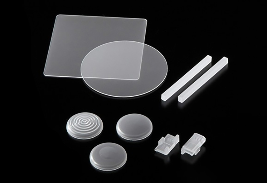
Introduction Dielectric substrates are indispensable materials in modern electronic devices. They play a crucial role in supporting circuits, optimizing electromagnetic performance, and protecting components. As technology advances, dielectric substrates have evolved to include a diverse range of materials with tailored properties, meeting the demands of various applications such as microwave circuits, antenna designs, and sensor...Continue Reading
1. Introduction Transparent Conductive Oxides (TCOs) are a unique class of materials that combine two essential properties: optical transparency and electrical conductivity. These characteristics make TCOs indispensable in various technological applications, ranging from touch screens and flat-panel displays to solar cells and smart windows. The ability to conduct electricity while allowing light to pass through...Continue Reading
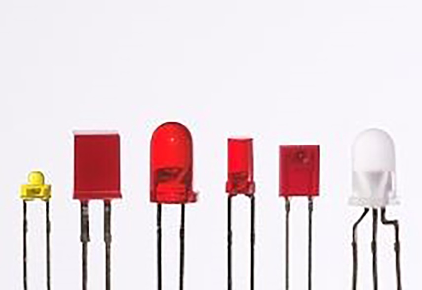
Thin-film transistors (TFTs) are fundamental components in a myriad of electronic devices that shape our daily lives, from the vibrant displays of smartphones and TVs to the essential functionality of touch screens and solar cells. Central to the fabrication of these versatile transistors is the use of magnesium oxide (MgO) targets, a critical material in...Continue Reading
Introduction Yttrium Iron Garnet (YIG), with its enigmatic presence in the domain of material science, has been silently powering some of the most advanced technologies of our time. Discovered in the mid-20th century, this ferrimagnetic material has evolved far beyond its initial applications, proving itself as a backbone in the realms of microwave and optical...Continue Reading
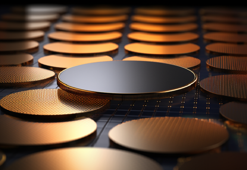
Introduction Gallium Arsenide (GaAs) wafers have revolutionized the world of semiconductor technology with their exceptional performance and unique properties. In this comprehensive guide, we will explore the power of GaAs wafers and delve into their applications, fabrication process, and key benefits. 1. Understanding GaAs Wafers: GaAs wafers are composed of gallium (Ga) and arsenic...Continue Reading
Introduction Semiconductor technology has been at the forefront of driving innovation in various industries, ranging from telecommunications and consumer electronics to renewable energy and aerospace. Within the realm of semiconductors, Gallium Arsenide (GaAs) wafers have emerged as a powerful tool, fueling advancements in semiconductor devices and enabling the development of cutting-edge technologies. In this article,...Continue Reading
Introduction Gallium Arsenide (GaAs) wafers are an essential component in the production of high-performance electronic devices, and they have specific specifications that must be met to ensure their effectiveness. In this article, we will discuss the key specifications of GaAs wafers so that you can have a further understanding of this useful material. What Are...Continue Reading
Introduction Gallium Arsenide (GaAs) wafers have a variety of applications in the field of electronics, particularly in the production of high-performance electronic devices. In this article, we will explore some common applications of GaAs wafers for electronic device manufacturing and provide a better understanding of their properties and advantages. Properties of Gallium Arsenide Wafer Gallium...Continue Reading