What is Chemical Vapor Deposition (CVD)? The Ultimate Guide
Introduction
Chemical Vapor Deposition (CVD) might sound like an obscure lab technique, but it’s the invisible engine behind modern technology. It’s what makes your smartphone processor faster, your new sunglasses more scratch-resistant, and a jet engine withstand infernal temperatures. In essence, CVD is the art of turning a gas into a perfect solid coating, and it’s one of the most versatile tools in modern manufacturing.
Here is a QUICK GUIDE for this article:
- Why CVD Matters: The Core Principles
- Two Chemical Vapor Deposition Reactors
- Types of Chemical Vapor Deposition Processes
- Benefits of Chemical Vapor Deposition: Why It’s So Widely Used
- CVD vs. PVD: A Quick Comparison
- Real-World Applications of CVD
- Frequently Asked Questions (FAQ)
- Navigating the CVD Landscape: A Practical Selection Guide
1. Why CVD Matters: The Core Principles
At its heart, CVD is a process where a solid material is deposited onto a surface from a gaseous state through chemical reactions. Imagine reactive gas molecules adsorbing and chemically bonding to an object, building up a layer atom by atom, but in a highly controlled vacuum chamber.
The basic steps, as detailed in your original introduction, are:
- Transport: One or more volatile precursors (the source materials) are transported into a reaction chamber.
- Reaction: These precursors react or decompose on a heated substrate surface.
- Deposition: A solid material forms and adheres to the substrate as a thin, high-quality film.
- Byproduct Removal: The chemical by-products and unreacted gases are emitted from the chamber.
This fundamental process can be tailored in numerous ways, leading to different types of CVD reactors and techniques.
2. Two Chemical Vapor Deposition Reactors
There are two types of CVD reactors, each with its own applications, advantages, and disadvantages.
Hot Wall Reactors
Hot wall reactors are less commonly used compared to other types. They involve heating both the substrates and the reactor walls.
Advantages
- Large batches of substrates can be produced at once.
- Hot wall reactors are easy to operate.
- There is a uniform substrate temperature. Hence, there is a uniform coating thickness.
- Hot wall reactors can operate at a wide range of temperatures and pressures.
Disadvantages
- It requires a very high temperature and energy.
- Coating occurs not only on the substrate but also on the reactor walls. This makes it difficult to clean the reactor.
- Gas-phase reactions are likely to occur.
Cold Wall Reactors
Cold wall reactors are the most commonly used type of CVD reactor. They heat the substrate while cooling the reactor walls. This creates a higher temperature on the substrate compared to the walls. Cold wall reactors are particularly suitable for compound semiconductor CVD processes.
Advantages
- There are fewer coatings on the walls, making cleaning easier.
- Cold-wall reactors require less temperature and energy.
- Cold-wall reactors support chemical vapor deposition processes that involve plasmas.
- Can achieve high deposition rates due to the high temperature gradient at the substrate surface.
- Gas-phase reactions are less likely to occur.
Disadvantages
- They are more difficult to operate.
- Fewer substrates can be worked on at once.
- The substrate temperature is not uniform. Hence, coating thickness is usually not uniform.
3. Types of Chemical Vapor Deposition Processes
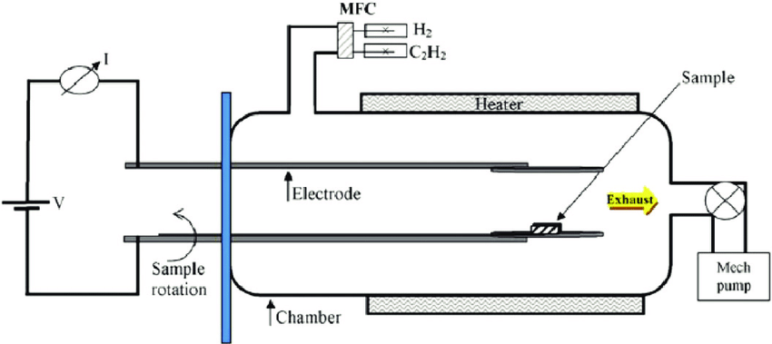
Plasma-enhanced Chemical Vapor Deposition (PECVD)
PECVD is a specialized form of chemical vapor deposition. In this method, the reactive gases are ionized into plasma using a combination of radio frequency or direct current discharge. This ionization process occurs within the space between two electrodes, where the gases are introduced and transformed into plasma. This technique enhances the deposition process by allowing the films to be deposited at lower temperatures compared to standard CVD methods.
Thermal Chemical Vapor Deposition
Thermal CVD relies primarily on thermal energy to drive the chemical reactions. It is commonly conducted at atmospheric pressure (APCVD), but low-pressure variants (LPCVD) are also widely used for improved uniformity. In this process, the precursor material is added to burning gas, making the precursor highly reactive. This method facilitates the deposition of thin films directly onto substrates at atmospheric pressure, utilizing the enhanced reactivity of the precursors facilitated by the heat from the burning gas to achieve efficient and uniform coatings.
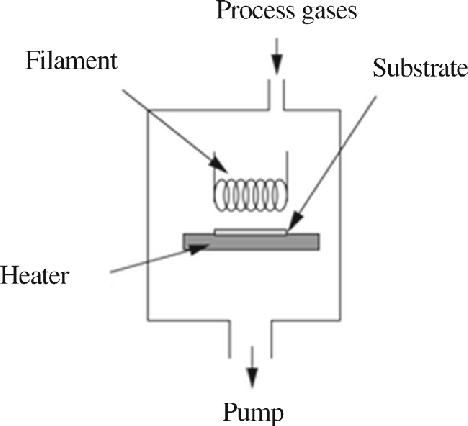
Hot-filament Chemical Vapor Deposition (HFCVD)
HFCVD, also known as catalytic chemical vapor deposition, utilizes a heated filament to decompose precursor gases. In this process, the hot filament serves as a catalyst, significantly enhancing the breakdown of the gases. Positioned above the substrate, which is maintained at a lower temperature compared to the filament, this method ensures efficient deposition of materials onto the substrate. The differential temperature between the hot filament and the cooler substrate facilitates a controlled deposition environment, leading to uniform and high-quality coatings.
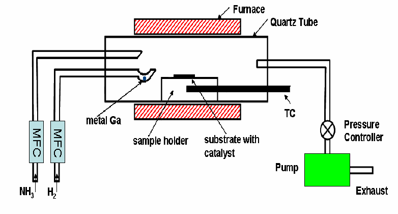
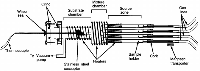
Metalorganic Chemical Vapor Deposition (MOCVD)
MOCVD is a specialized technique extensively used for depositing single or polycrystalline thin films. Unlike molecular beam epitaxy, which involves physical deposition to grow crystals, MOCVD operates through chemical reactions. In this process, metalorganic compounds (e.g., trimethylgallium) are used alongside hydride or other precursors (e.g., ammonia, phosphine) to deposit compound semiconductors. These chemical compounds undergo decomposition under controlled conditions, leading to the formation of thin film materials on substrates. This distinction emphasizes MOCVD’s role in facilitating complex chemical transformations essential for the production of advanced material coatings.
Laser Chemical Vapor Deposition (LCVD)
LCVD is a precise method commonly utilized for spot coating applications, especially in the semiconductor industry. This technique employs a focused laser beam to selectively heat specific areas of a substrate. The localized heating by the laser accelerates the deposition process on the heated areas, allowing for rapid and controlled growth of material coatings. This targeted approach ensures high precision in coating placement and thickness, making LCVD ideal for applications requiring meticulous material deposition on complex substrate geometries.
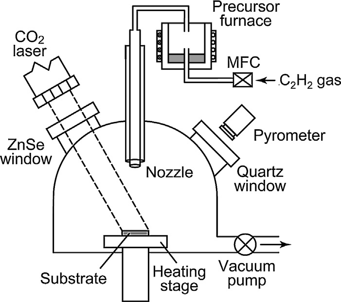
Yu, Shu & Tu, Rong & Goto, Takashi. (2015). Preparation of SiOC nanocomposite films by laser chemical vapor deposition. Journal of the European Ceramic Society. 36. 10.1016/j.jeurceramsoc.2015.10.029.
4. Benefits of Chemical Vapor Deposition: Why It’s So Widely Used
Chemical Vapor Deposition (CVD) is a widely used method for applying thin films to surfaces, and its popularity stems from several key advantages that make it suitable for various industrial applications. Here are some expanded insights into the benefits of using CVD:
- Affordability: CVD is recognized for being a cost-effective coating method compared to other deposition techniques. Its efficiency and ability to operate at scale reduce overall manufacturing costs, making it an economically viable option for both high-volume production and specialized applications where cost containment is crucial.
- Versatility: One of the standout features of CVD is its versatility. This method is capable of depositing a wide range of materials, including metals, ceramics, and polymers, onto virtually any substrate. This flexibility makes it invaluable in industries ranging from aerospace to electronics, where it is used for depositing everything from protective coatings to conductive layers.
- High Deposition Rate: CVD processes are particularly noted for their high deposition rates, enabling rapid coating of substrates, which is a significant advantage in mass production settings. This efficiency ensures that large batches of components can be processed quickly, enhancing throughput and reducing turnaround times.
- Uniform Coating: The ability to provide a consistent, uniform coating over the entire surface of a substrate, including complex geometries and varying scales, is another benefit of CVD. This uniformity is critical in applications where the precise thickness of a coating influences the performance or durability of the end product, such as in semiconductor manufacturing or protective coatings in aerospace components.
- High Purity: Chemical vapor-deposited materials are typically of very high purity, as the process involves the deposition of vapor-phase precursors that can be carefully controlled and purified before use. This results in coatings free from impurities that could compromise the structural integrity or functionality of the coating.
- Non-Line of Sight Deposition: Unlike line-of-sight processes, CVD can coat complex shapes and internal surfaces that are not directly exposed to the source of the deposition material. This capability is particularly important for components with intricate designs or internal cavities that require consistent coverage, such as parts used in fluid flow systems or complex electronic devices.
Further Reading: Table Comparison: Physical Vapor Deposition Vs. Chemical Vapor Deposition
5. CVD vs. PVD: A Quick Comparison
A common question is how CVD differs from Physical Vapor Deposition (PVD). Here’s a high-level comparison to help clarify:
| Feature | Chemical Vapor Deposition (CVD) | Physical Vapor Deposition (PVD) |
|---|---|---|
| Process | Chemical reaction from gaseous precursors. | Physical ejection (sputtering, evaporation) of solid source. |
| Coating Direction | Omnidirectional (excellent for complex shapes). | Line-of-sight (shadows may not be coated). |
| Film Properties | Excellent conformity, high purity, strong adhesion. | High hardness, smooth surface, compressive stress. |
| Temperature | Typically high (can exceed 900°C). | Typically low (often below 500°C). |
| Cost (dependent on application) | Generally more cost-effective for high-volume, complex parts. | Can be more economical for simpler, temperature-sensitive substrates. |
Choosing Between Them: Use CVD when you need to coat complex geometries with uniform, high-purity films and high temperature is not an issue. Use PVD for temperature-sensitive materials or when you require very specific mechanical or optical properties on less complex shapes.
6. Real-World Applications of CVD
Electronics
In electronics, CVD plays a pivotal role in semiconductor fabrication, where it is employed to deposit thin films that are essential for the manufacturing of integrated circuits and transistors. These thin films form the active layers and gate dielectrics crucial for the function of electronic devices. The ability of CVD to create uniform and defect-free layers with high precision makes it indispensable in producing the increasingly miniaturized components required for advanced electronics.
Further Reading: CVD Technology’s Impact on Semiconductor Thin Film Production
Cutting Tools
Chemical vapor deposition is extensively used in the tool-making industry to coat cutting tools, such as drills and milling cutters. The CVD coatings, typically made from materials like titanium nitride or diamond-like carbon, significantly enhance the durability, efficiency, and performance of these tools. These coatings reduce tool wear and corrosion, improve lubricity to reduce friction, and provide a thermal barrier that helps in maintaining the tool’s integrity under high-heat conditions. This leads to longer tool life, greater precision in machining, and reduced downtime for tool replacement.
Solar Cells
Chemical Vapor Deposition is indispensable in both mainstream and next-generation photovoltaic technology, primarily for depositing critical thin-film layers that enhance light management and device efficiency.
In the dominant crystalline silicon (c-Si) solar cell industry, Plasma-Enhanced CVD (PECVD) is the standard technique for depositing high-quality silicon nitride (SiNₓ:H) films. These films serve a dual purpose: as an excellent anti-reflection coating to minimize light loss, and as a superior surface passivation layer to reduce charge recombination, directly boosting cell conversion efficiency.
For emerging thin-film and perovskite solar cells, CVD techniques enable precise deposition of key functional layers. This includes transparent conductive oxides (TCOs) as front electrodes, buffer layers, and the intricate perovskite absorber layers themselves. The excellent conformity and compositional control offered by variants like Atomic Layer Deposition (ALD, a subtype of CVD) are particularly valuable for creating uniform, pinhole-free films on textured surfaces or within complex tandem cell architectures, which is crucial for both performance and long-term stability.
7. Frequently Asked Questions (FAQ)
Q: What are the main disadvantages of CVD?
A: The primary drawbacks include high process temperatures that can damage sensitive materials, the use of hazardous and expensive precursor gases, and the production of toxic byproducts that require careful handling and disposal.
Q: What materials can be deposited using CVD?
A: A wide variety, including silicon, germanium, tungsten, titanium nitride, silicon dioxide, silicon carbide, diamond-like carbon, and many compound semiconductors.
Q: Is CVD more expensive than PVD?
A: It depends on the application. CVD often has higher precursor and energy costs, but can be more cost-effective for coating complex parts in a single run due to its superior coverage. PVD may be cheaper for simpler, temperature-sensitive components.
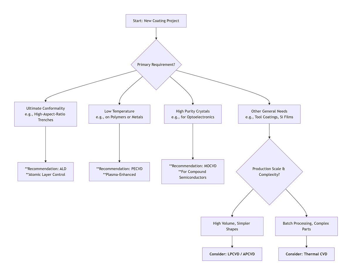
8. Navigating the CVD Landscape: A Practical Selection Guide
A Practical Framework for Selecting a CVD Process
Understanding the types of CVD is one thing; choosing the right one for your specific project is another. The following flowchart provides a high-level decision-making framework based on key application requirements:
Key Questions to Ask Your Materials Supplier:
The success of any CVD process hinges on the quality of its precursors. When sourcing materials, consider discussing these points with your supplier:
-
Purity & Consistency: What is the guaranteed purity (e.g., 5N, 6N)? How do you ensure batch-to-batch consistency in composition and evaporation rates?
-
Technical Data: Can you provide detailed specifications on decomposition temperature, vapor pressure, and recommended carrier gases?
-
Application Support: Do you have experience or data for this material in applications like [mention your field, e.g., semiconductor dielectrics, hard coatings]?
-
Safety & Handling: What are the specific handling procedures, storage conditions, and disposal recommendations for this precursor?
Frontiers of CVD Technology
CVD continues to evolve, enabling the next generation of materials:
-
Synthesis of 2D Materials: CVD is the leading method for producing large-area graphene, hexagonal boron nitride (h-BN), and transition metal dichalcogenides (like MoS₂). The focus is on achieving defect-free, single-crystal monolayers, which requires ultra-precise control over parameters and high-purity, specialized precursors.
-
Sustainable Manufacturing: The industry is actively working to reduce its environmental impact through safer precursor alternatives, process intensification to reduce waste and energy use, and advanced byproduct abatement systems.
9. Conclusion
Chemical Vapor Deposition (CVD) is a crucial technique in thin film deposition, renowned for its versatility and broad application across industries such as electronics, cutting tools, and solar cell manufacturing. It combines affordability, high deposition rates, and the ability to produce uniform, high-purity coatings, making it essential for both mass production and specialized applications. As technology advances, ongoing research is enhancing CVD’s capabilities even further. For more detailed insights into CVD and its applications, visit https://www.sputtertargets.net/.


