An Overview of Sputtering Deposition
What is Sputtering Deposition?
Sputtering deposition, or sputter coating, is one of the physical vapor deposition technology, whereby particles are ejected from a solid target material due to the bombardment of the target by energetic particles.
It is an electronic process that deposits thin films of metals or other materials onto a variety of surfaces. Most often, sputtering is used to apply thin platings onto silicon wafers, solar panels, and display screens.
How Does Sputtering Deposition Work?
The sputtering deposition is done in a vacuum chamber into which an inert gas is introduced, and the most used is argon ions. Two items are placed into that chamber: the item to be plated, which is also called the “substrate”, and the material that will be applied, which is also called the “sputtering target”.
After ionizing the argon, the argon ions acquire kinetic energy under the acceleration of the electric field and bombard the target. The atomic migration of the target surface can only be achieved when the argon-ion energy reaches the binding energy of the target electrode (about the sublimation heat of the target material). When the energy of the bombardment particle exceeds four times the sublimation heat of the target material, the atom is pushed out of the lattice position and becomes the gas phase and escapes from the target material, and travels to the material to be coated. This process is called sputtering. For most metals, the sputtering threshold energy is about 10 to 25 electron volts.

In short, the basic principles of sputtering deposition can be divided into three process steps:
(1) Gasification of the plating material: sputtering
(2) Migration of plating atoms, molecules, or ions: a variety of reactions occurs after the collision of atoms, molecules or ions.
(3) The plating atoms, molecules, or ions are deposited on the substrate.
What Types of Materials Can Be Used in Sputtering Deposition?
The sputtering targets come in a wide variety of sizes and materials, including pure metal sputtering targets, ceramic sputtering targets, and alloy sputtering targets. And their purities range from commercial-grade 99.9% purity to the highest, 99.999% zone refined Ultra-Pure grade.
What are the Forms of Sputtering Deposition?
There are many forms of sputtering deposition, and here are some of them.
* Magnetron sputtering uses a magnetic field to control plasma bombardment of the target to increase plasma density. Magnetron sputtering has the advantages of high speed, low temperature, and low damage.
* UBM sputtering is an abbreviation for unbalanced magnetron sputtering. The enhanced field coil is used to enhance the plasma density near the workpiece. UBM can achieve a denser coating. However, the energy used in the UBM process is higher, so the temperature will rise accordingly.
* Dual target magnetron sputtering (DMS) is a technique used to deposit insulator coatings. Instead of using direct current (DC) between the cathode and the vacuum chamber, alternating current (AC) is used between the two cathodes. DMS is used for magnetron sputtering of high-speed deposition such as preparing oxide coatings.
What are the Advantages of Sputtering?
Good Durability
The film obtained by sputtering deposition is sometimes harder and more resistant to corrosion.
Wide Application
Nearly all types of inorganic and some organic coating materials can be used on many groups of substrates and surfaces using a wide variety of finishes.
Environmentally friendly
Since the process of sputter deposition happens in a vacuum environment, it is more environmentally friendly than other traditional coating techniques such as electroplating and painting. And the sputtering process won’t produce poisonous gas such as CO or SO2.
Convenient cleaning
You can save the time and cost of cleaning and polishing general copper (gold) products, and a soft cloth or glass cleaner is sufficient to clean the sputter-coated film.
High-quality and multiple choices
The sputtered film has a wide variety of colors, and the surface is fine and smooth, rich in metallic luster, and never fades. Common colors are golden yellow (TiN), bright silver (CrN), purple (TiAlN), and so on.
What are the Uses of Sputtering Deposition?
Sputtering targets have important applications in many areas. There are some differences in the selection and performance requirements of sputtering materials in different application fields. Among them, anelva targets, the sputtering targets used in semiconductor integrated circuits, are the most demanding and strict.
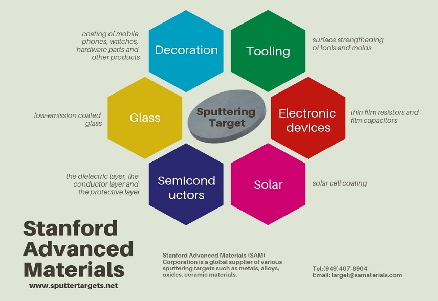
We have summarized the main types, applications, and performance requirements for sputtering targets used in the several mentioned fields.
| Type | Application | Main Variety | Performance Requirement |
| Semiconductor | Used to prepare integrated circuit core materials | W, WTi, Ti, Ta, Al alloy with purity 4N or 5N. | Highest technical requirements; ultra-high purity metal; high precision size; high integration |
| Flat display | Sputtering technology guarantees uniformity of film produced increases productivity, and reduces costs | Nb, Si, Cr, Mo, MoNb, Al alloy, Cu, and Cu alloy targets | High technical requirements; high purity materials; large material area; high uniformity |
| Decoration | Used for coating the surface of the product for beautification, wear resistance, and corrosion resistance. | Cr, Ti, Zr, Ni, W, TiAl, CrSi, CrTi, CrAlZr target | General technical requirements; mainly used for decoration, energy saving, etc. |
| Tool | Enhance the surface of tools and molds, improve the life and the quality of the parts manufactured | TiAl, CrAl, Cr, Ti, TiC, Al2O3 target | High-performance requirements; extended service life |
| Solar | Sputter coating technology for the production of fourth-generation thin-film solar cells | ZnOAl, ZnO, ZnAl, Mo, CdS, CIGS target | High technical requirements; large application range |
| Electron device | Thin film resistors, film capacitors | NiCr, NiCrSi, CrSi, Ta, NiCrAl target | Requires small size, good stability, and low-temperature coefficient of resistance |
Conclusion
Thank you for reading our article and we hope that it can help you have a better understanding of sputtering deposition. This is just a very basic overview of sputtering deposition. If you are not sure which kind of sputtering is taking place on your production line, please contact us. If you want to purchase a specific type of sputtering target, please send us an inquiry. For more information, please visit https://www.sputtertargets.net/.


