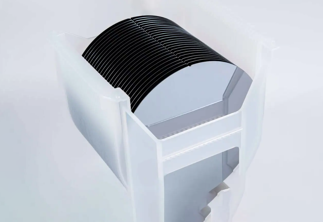
I. Introduction Silicon-on-insulator (SOI) technology represents a pivotal advancement in semiconductor manufacturing, offering enhanced performance and efficiency over traditional bulk silicon approaches. By integrating a thin silicon layer atop an insulating substrate, SOI facilitates superior electrical isolation and reduced parasitic capacitance, which is critical for high-performance electronic devices. SOI involves layering a silicon wafer on...Continue Reading
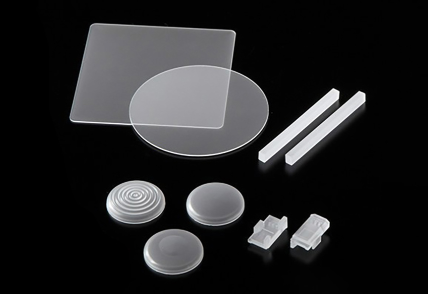
Introduction Dielectric substrates are indispensable materials in modern electronic devices. They play a crucial role in supporting circuits, optimizing electromagnetic performance, and protecting components. As technology advances, dielectric substrates have evolved to include a diverse range of materials with tailored properties, meeting the demands of various applications such as microwave circuits, antenna designs, and sensor...Continue Reading
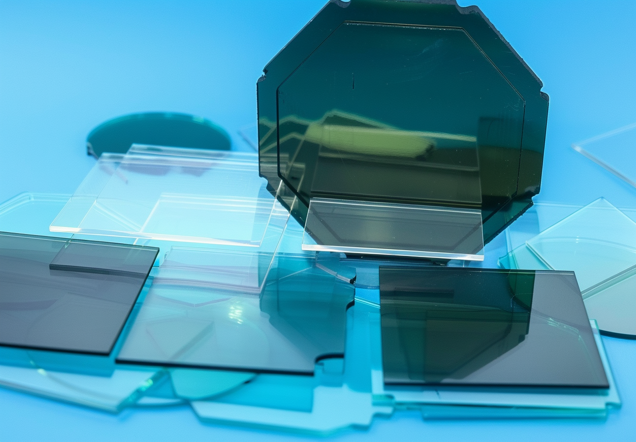
Silicon carbide (SiC) crystal substrates are advanced semiconductor materials with unique properties. These substrates have become popular because they perform better than traditional silicon in many areas. SiC has a structure with alternating layers of silicon and carbon atoms. This structure gives SiC its strength and versatility, making it perfect for use in electronics, optoelectronics,...Continue Reading
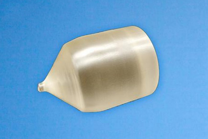
Introduction Synthetic diamonds, particularly those produced by Chemical Vapor Deposition (CVD), represent a significant technological advancement that blends centuries of curiosity and modern scientific ingenuity. Historically, diamonds have been highly sought after not only for their aesthetic value but also for their remarkable physical properties. Researchers like Isaac Newton have studied these properties, paving the...Continue Reading
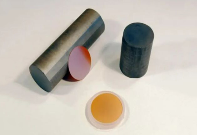
Introduction Yttrium Iron Garnet (YIG), with its enigmatic presence in the domain of material science, has been silently powering some of the most advanced technologies of our time. Discovered in the mid-20th century, this ferrimagnetic material has evolved far beyond its initial applications, proving itself as a backbone in the realms of microwave and optical...Continue Reading
Introduction Gallium Arsenide (GaAs) wafers have a variety of applications in the field of electronics, particularly in the production of high-performance electronic devices. In this article, we will explore some common applications of GaAs wafers for electronic device manufacturing and provide a better understanding of their properties and advantages. Properties of Gallium Arsenide Wafer Gallium...Continue Reading
Introduction Gallium phosphide (GaP) is a compound semiconductor material that has gained increasing attention in the semiconductor industry. GaP wafers offer several advantages over traditional silicon wafers, including high efficiency, high-speed operation, and high power handling capabilities. In this article, we will talk about the benefits of using gallium phosphide wafers in electronic and...Continue Reading
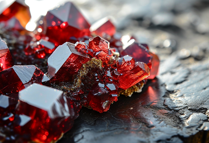
Introduction Garnets (A3B2(SiO4)3) are a group of minerals commonly used as substrates, abrasives, and gemstones. Garnets share similar physical properties and crystal structures, yet they have disparities in chemical composition. Here, this article is going to explore the garnet family in the specific case of gadolinium gallium garnet. Hope that you can have a basic...Continue Reading