An Overview of Magnetron Sputtering
An Overview of Magnetron Sputtering
Magnetron sputtering, a physical vapor deposition (PVD) process, is a main thin film deposition method for manufacturing semiconductors, disk drives, CDs, and optical devices. Magnetron sputtering has the advantages of high speed, low temperature, and low damage. In this article, let’s take a look at the definition, working principle, and applications of the magnetron sputtering coating method.
Definition of Magnetron Sputtering
Sputter deposition is the process whereby particles of the sputtering materials are sputtered out and deposited on a substrate to form a film. Since ions are charged particles, we can add magnetic fields to control their speed and behavior. And that’s where its name “magnetron sputtering” comes from.
Features of Magnetron Sputtering
The first magnetron sputtering source with a patent filed is a planar magnetron sputtering source invented by John S. Chapin in 1974. At that time, although conventional diode sputtering can deposit extremely thin films down to the atomic scale, its sputtering speed is slow and it only works for small-area coating. Besides, the bombardment of the substrate can also create overheating or damage to the object to be coated.
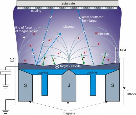
Magnetron sputtering deposition uses electrons behind the negative cathode to trap electrons on the negatively charged target material. The magnetic field constraints on the charged particles increase the plasma density, allowing a faster deposition rate.
Working Principle of Magnetron Sputtering
Under the action of an electric field of several hundred to several thousand electron volts, the plasma is accelerated and obtained sufficient force to bombard the cathode, causing the atoms of the solid sputtering target to be ejected in a typical line-of-sight cosine distribution. These atoms will condense on the surface of the substrate to form a thin film.
Types of Magnetron Sputtering Sources
Magnetron sputtering sources are divided into balanced and unbalanced. The coating of the balanced magnetron sputtering source is uniform, and the coating of the unbalanced magnetron sputtering source has a strong bonding force. The balanced type is mostly used for semiconductor optical films, and the unbalanced type is mostly used for wear decorative films.
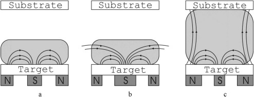
b. Type-1 Unbalanced Magnetron
c. Type-2 Unbalanced Magnetron
Materials Used in Magnetron Sputtering
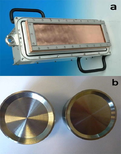
Planar targets and rotatory targets are the most common magnetron sputtering cathode. The advantages and disadvantages of these two types of sputtering targets are not obvious, but they do have different applied areas. Planar magnetrons are preferred in larger-scale systems where substrates scan linearly past the targets on some type of conveyor belt or carrier. Rotatory sputtering magnetrons are more frequently found in smaller-scale batch systems or single-wafer stations.
b. rotatory magnetron
Application of Magnetron Sputtering
- Various functional films: films having special functions such as absorption, transmission, reflection, refraction, and polarization. For example, a low-temperature deposition silicon nitride anti-reflection film for improving the photoelectric conversion efficiency of a solar cell.
- Applications in decorative fields such as various total reflection films and translucent films, mobile phone cases, and mice.
- In the field of microelectronics, it can be used as a non-thermal coating technology, mainly in chemical vapor deposition (CVD), to obtain a uniform film with a large area.
- Optics field: IF closed field unbalanced magnetron sputtering technology has been applied in optical films (such as antireflection film), low-emissivity glass, and transparent conductive glass.
- In the machining industry, the surface deposition technology of surface functional film, super hard film, and self-lubricating film has been greatly developed since its inception. These films can effectively improve surface hardness, composite toughness, wear resistance, and high-temperature chemical stability, and the service life of coated products.
In addition to the above fields, magnetron sputtering also plays an important role in the research of high-temperature superconducting thin films, ferroelectric thin films, giant magnetoresistive thin films, thin-film luminescent materials, solar cells, and memory alloy thin films.
Thank you for reading our article and we hope you’ve enjoyed it. If you want to know more about magnetron sputtering and other film coating methods, we would like to recommend you visit Stanford Advanced Materials for more information.
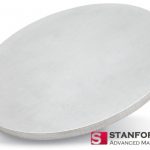
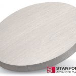
Popular Sputtering Target Used in Ion Beam Sputtering
Titanium (Ti) Sputtering Target
 Tungsten (W) Sputtering Target
 Tantalum (Ta) Sputtering Target


