Chemical Formula: SiO2
Catalog Number: ST0185
CAS Number: 7631-86-9
Purity: 99.9%, 99.95%, 99.99%, 99.995%
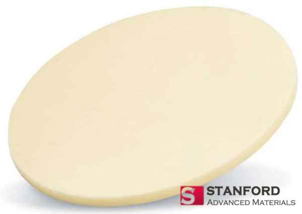
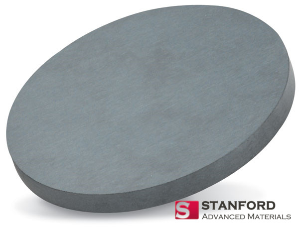
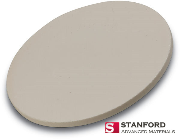
Shape: Discs, Plates, Column Targets, Step Targets, Custom-made
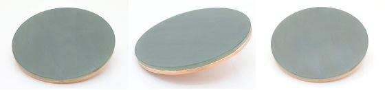
Silicon dioxide sputtering targets are available in various forms, purities, sizes, and prices. Stanford Advanced Materials (SAM) offers high-quality SiO2 sputter targets at the most competitive price.
 Silicon Oxide Sputtering Target Safety Data Sheet
High-Purity SiO2 Sputtering Target for Advanced Thin Film Applications
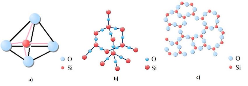
Silicon dioxide sputtering target from Stanford Advanced Materials contains Si and O. Silicon dioxide (SiO2), also known as Silica, is a natural compound made from two of the most abundant materials on the planet: silicon (Si) and oxygen (O2). Silica is most commonly considered to be in the form of quartz. It exists naturally in water, plants, animals and the earth. 59% of the earth’s crust is composed of silicon dioxide. In addition, it also forms more than 95% of the known rocks on Earth. Here is the structure of SiO2.
Key Features:
| Material Type | Silicon (IV) Oxide |
| Symbol | SiO2 |
| Color/Appearance | White, Crystalline Solid |
| Melting Point (°C) | 1,610 |
| Boiling Point (°C) | 2,230 |
| Density (kg/m-3) | 2,533 |
| Sputter | RF |
| Type of Bond | Copper, Indium, Elastomer |
| Comments | Quartz is excellent in E-beam. |
| Available Sizes | Dia.: 1.0″, 2.0″, 3.0″, 4.0″, 5.0″, 6.0″ Thick: 0.125″, 0.250″ |
We also offer other customized shapes and sizes of the sputtering targets. Please send us an inquiry for more information.
SiO2 sputtering materials are commonly available with indium bonding and elastomer bonding options. Copper bonding is also widely used and can be customized based on customer requirements. Stanford Advanced Materials specializes in machining standard backing plates and collaborates with Taiwan Bonding Company to provide comprehensive bonding services. For inquiries about target bonding materials, methods, and services, please click here.
Our silicon oxide sputtering targets are tagged and labeled externally for efficient identification and quality control. They are vacuum-packed to prevent moisture absorption and carefully cushioned to avoid damage during storage and transportation.
High-quality silicon dioxide sputtering targets are available in various forms, purities, sizes, and prices. We specialize in producing high-purity thin film coating materials with the highest possible density and smallest possible average grain sizes for use in semiconductor, chemical vapor deposition (CVD), and physical vapor deposition (PVD) display and optical applications. Please send us an inquiry for current pricing on sputtering targets and other deposition materials not listed.
Q1: What purity levels are available for silicon dioxide sputtering targets?
Purity levels typically range from 99.9% to 99.995%, ensuring high-quality thin films.
Q2: How is the silicon dioxide sputtering target packaged?
Targets are vacuum-sealed or moisture-proof packed to protect against damage and contamination.
Q3: Can silicon dioxide sputtering targets be customized?
Yes, sizes, shapes, and bonding types can be tailored to meet specific application needs.
Q4: Can SiO₂ be deposited using DC sputtering?
Not ideal. SiO₂ is a dielectric, so it tends to accumulate charge under DC sputtering. RF sputtering is the better option for stable, uniform growth.
Q5. Can SiO₂ form epitaxial films? On what substrates?
Yes, under the right conditions. Compatible substrates include silicon (Si), gallium arsenide (GaAs), aluminum (Al), and gallium nitride (GaN).
Q6. Where are SiO₂ thin films used?
They show up in everything from semiconductors and solar cells to optical lenses, displays, drug delivery systems, implants, and data storage like CDs and DVDs.
Submit your review | |
I needed sputtering targets for a experiment project, and these little guys did not disappoint me. Satisfied with SAM's products.