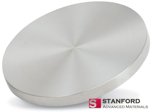
Zirconium Sputtering Targets in Semiconductor Chip Manufacturing
Introduction
The semiconductor industry is driving the technological revolution, fueling the progress of electronics, computing, and communications. As performance demands rise and chip dimensions continue to be reduced, the material employed for their manufacture must conform to increasingly stringent specifications. High-purity zirconium sputtering targets have become a flagship material for the industry, making it possible to form high-quality metal oxide thin films, gate material, as well as metal interconnect layers. This article focuses on the utilitarian applications of zirconium sputtering targets in semiconductor manufacturing and how useful they are in solving industry problems and technological innovation.
Before getting into the specific applications, there is a need to briefly outline the characteristics that make zirconium an ideal candidate to be manufacturing in semiconductors:
- High Purity: Zirconium sputtering targets achieve purities of 99.995% or higher, ensuring minimal contamination during the deposition of thin films.
- Thermal Stability: Zirconium’s melting point is 1852°C and hence it is thermally stable in semiconductor processing’s high-temperature environment.
- Corrosion Resistance: Zirconium‘s superior chemical resistance means that the films it forms are durable.
- Excellent Uniformity of Films: Zirconium targets are capable of depositing dense, uniform, and defect-free films for next-generation semiconductor devices.
All these features make zirconium sputtering targets vital for a variety of thin-film applications in semiconductor manufacturing.
Their uses can be better explained by looking at their applications in some semiconductor chip fabrication processes. We discuss here three prominent application areas: metal oxide thin films, gate materials, and metal interconnect layers. We also look into other electronic and optoelectronic devices’ applications.
1. Metal Oxide Thin Films
Problem:
As semiconductor devices shrink in size, standard silicon dioxide (SiO₂) dielectric films are limited by factors such as increased leakage currents and absence of capacitance density.
Solution:
High-purity zirconium sputtering targets are employed to deposit zirconium oxide-based metal thin films, like zirconium dioxide (ZrO₂), using magnetron sputtering. ZrO₂ is a high-k dielectric whose dielectric constant is much higher compared to SiO₂ and thus applicable to future semiconductor nodes.
Applications and Benefits:
MOSFET Devices: ZrO₂ thin films are also used as gate dielectrics in MOSFETs, which reduce power consumption and improve energy efficiency by reducing leakage currents. It is particularly critical for low-power devices like smartphones and IoT sensors.
Capacitors: Zirconium oxides are also used in capacitors for increased capacitance density to enable smaller memory devices and power management systems.
Core Benefit: The ability of thin, high-quality, uniform dielectric layer manufacturing with zirconium sputtering targets allows manufacturers to meet the requirements of low–power and high–performance semiconductor devices.
2. Gate Materials
Problem:
With the shrinking of transistors, gate materials must meet higher requirements of thermal stability, electrical conductivity, and integration with high-k dielectrics. Traditional materials like polysilicon fall short for advanced nodes.
Solution:
High-purity zirconium sputtering targets allow the deposition of zirconium-based gate thin films used for gate material. These thin films possess superior thermal stability, low resistivity, and superior compatibility with high-k dielectrics like ZrO₂.
Applications and Advantages:
Future Transistor Architectures: Advanced transistor architectures such as FinFETs and gate-all-around (GAA) transistors are ensured by zirconium-based gate materials to have strong operation at nanoscale sizes.
High-Temperature Processing: The thermal stability of zirconium allows it to withstand high-temperature annealing steps in transistor manufacturing.
Core Advantage: With gate materials made of zirconium, chipmakers can switch faster and use less power, keeping up with the performance demands of AI processors, data center chips, and other emerging applications.
3. Metal Interconnect Layers: Increasing Reliability and Longevity
Problem:
With enhanced complexity in chip designs, metal interconnect layers become a key issue. The most widely used material for interconnects, copper, suffers from diffusion and electromigration and thus leads to long-term performance degradation.
Solution:
Thin films based on zirconium used as diffusion barriers and interconnect materials are deposited from zirconium sputtering targets. These films inhibit copper diffusion and enhance interconnect structure reliability.
Applications and Benefits:
Diffusion Barriers: Zirconium thin films are effective barriers between copper and neighboring materials, ensuring the integrity of interconnect layers.
Resistance to Electromigration: Zirconium‘s high melting point and electromigration resistance improve the durability of the interconnects, especially in high-performance autonomous vehicle chips and 5G networks.
Key Benefit: By improving interconnect layer performance and reliability, zirconium sputtering targets help to develop more durable semiconductor devices.
4. Other Applications in Electronics and Optoelectronics
Apart from traditional semiconductor applications, zirconium sputtering targets are used in other areas of electronics and optoelectronics where their unique characteristics enable innovative device configurations.
Applications and Advantages:
Transparent Conductive Films: Transparent films consisting of zirconium are used in displays and touchscreens with high transmissivity and better electrical conductivity.
Sensors and Actuators: Thin films of zirconium oxide are applied in gas sensors and biosensors due to their ultra-high sensitivity and stability. These sensors are most critical for environmental monitoring and medical diagnosis.
Optoelectronic Devices: Thin films of zirconium also find application in photodetectors and light-emitting devices, where they increase the optical performance as well as efficiency of the device.
Core Benefit: The thin film quality of zirconium allows for the production of extremely sophisticated electronic and optoelectronic devices for next-generation applications.
Conclusion
Pure zirconium sputtering targets are the essence of semiconductor manufacture, addressing significant issues in producing thin metal oxide films, gate components, and metal interconnect layers. Their unique properties, such as high purity, thermal stability, and corrosion resistance, enable the production of smaller, faster, and more reliable semiconductor devices. As the technology keeps evolving and pushes the boundaries of what is possible, the zirconium sputtering targets will remain an essential material, driving innovation in electronics, optoelectronics, and beyond.
Visit Stanford Advanced Materials’ homepage to see more sputtering target products.


