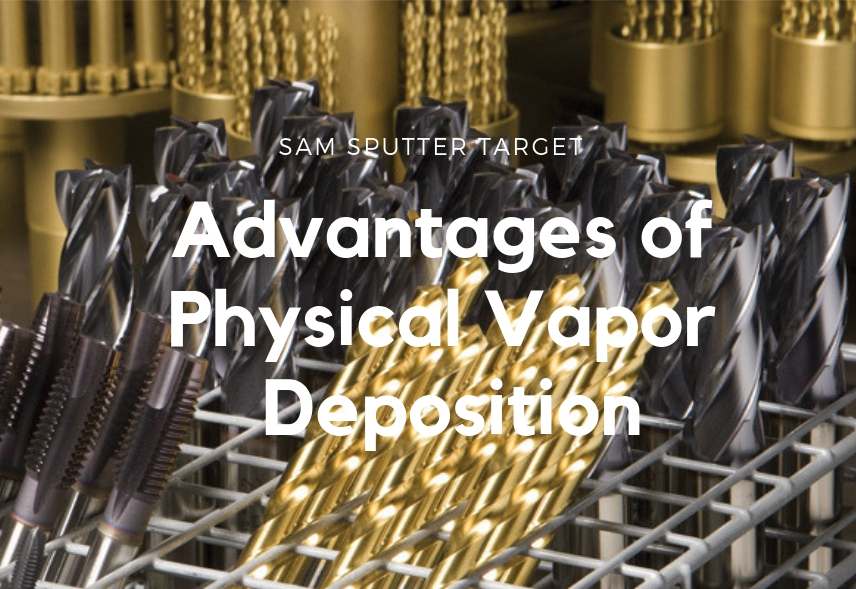
Introduction to PVD Coatings Physical Vapor Deposition (PVD) stands at the forefront of surface coating technologies, widely embraced by industries such as watches, jewelry, and automotive for its profound impact on product durability, aesthetics, and performance. This method distinguishes itself through its ability to offer coatings that are not only remarkably hard and corrosion-resistant but...Continue Reading
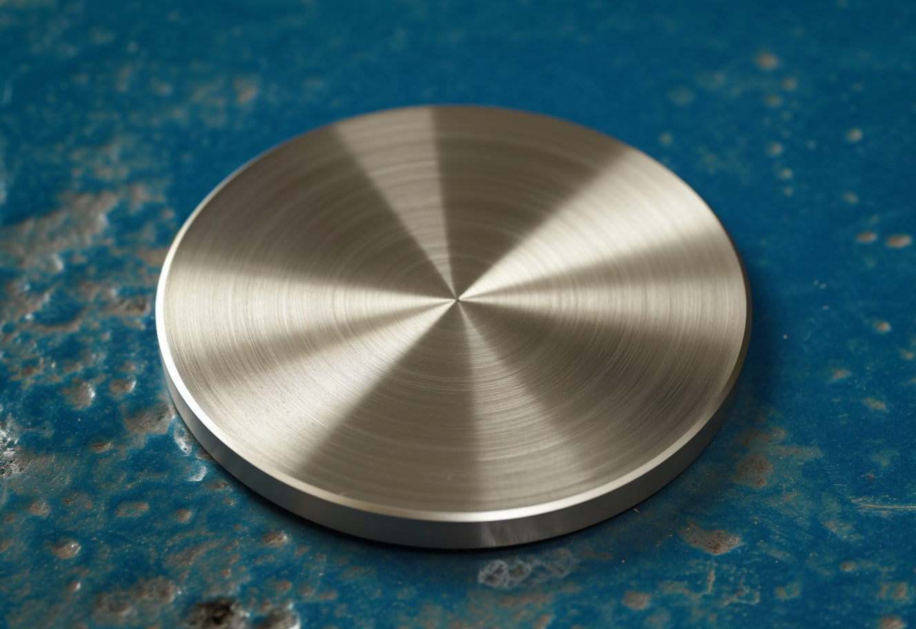
If you’ve ever wondered about the magic behind the shiny surfaces of electronic devices, solar cells, or even reflective mirrors, you might find the answer in a small but crucial component: the silver sputter target. In this article, we’ll break down the basics of silver targets, exploring what they are, how they work, and the...Continue Reading
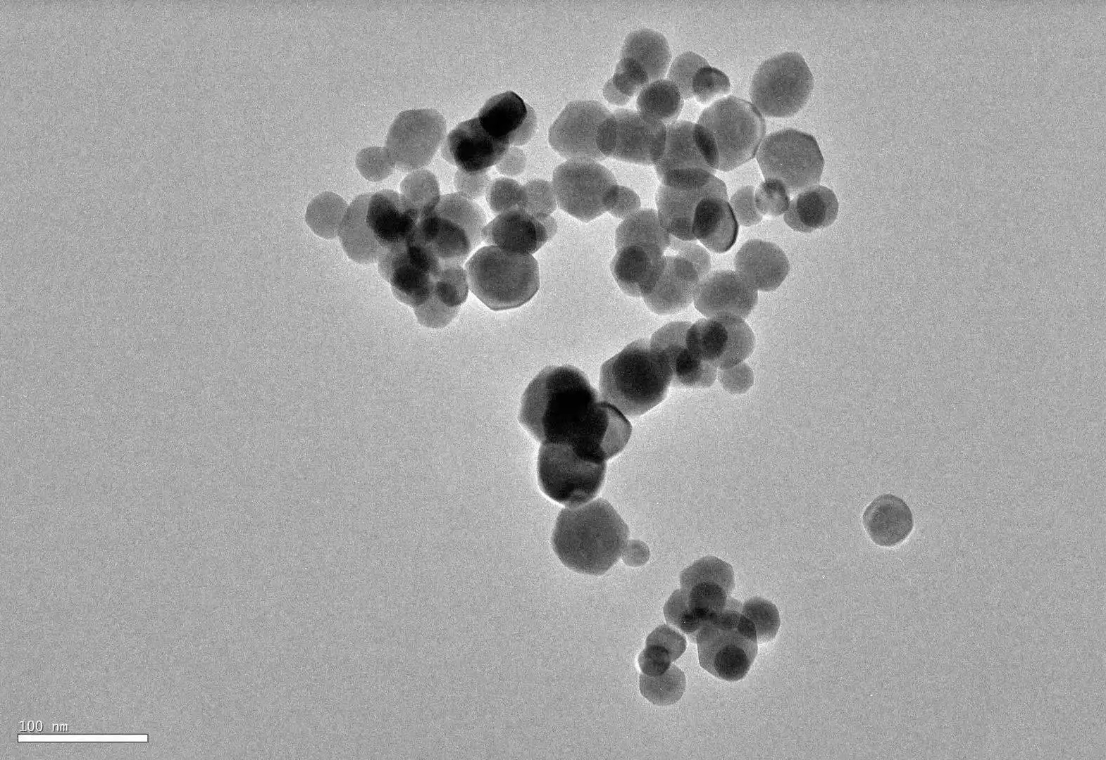
Introduction Indium Tin Oxide (ITO) has long been a stalwart in the realm of transparent conducting oxides, but recent strides in nanotechnology have ushered in a new era for this versatile material. This article looks at ITO nanotechnology, studying how making tiny structures is changing the way ITO works. This helps it do more things...Continue Reading
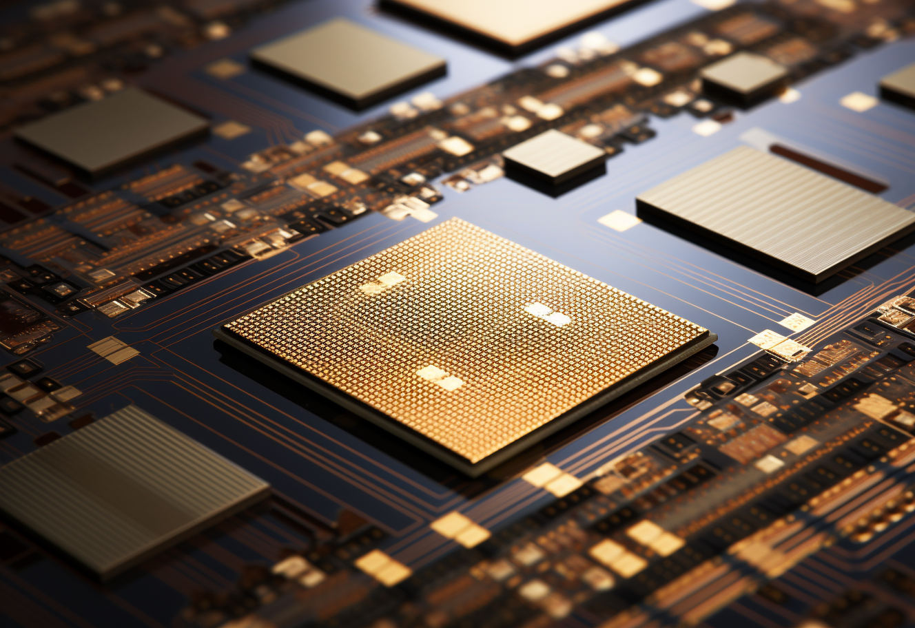
Introduction In the rapidly advancing landscape of semiconductor technology, Physical Vapor Deposition (PVD) stands as a pivotal tool for achieving precision and efficiency in thin film deposition processes. This article is a comprehensive exploration of the advanced applications of PVD technology within the semiconductor industry, offering a detailed examination of its diverse applications, supported by...Continue Reading
Introduction Thin-film deposition techniques play a crucial role in various industries, providing protective coatings that enhance the properties of materials. Among these methods, Physical Vapor Deposition (PVD) and Chemical Vapor Deposition (CVD) stand out, each distinguished by their unique characteristics, including the temperature at which they operate. Temperature Difference in PVD Definition and Basic Principles PVD encompasses...Continue Reading
Introduction Thin film coatings are a critical component of various industries, from microelectronics to optics. Two prominent techniques for depositing these thin films are sputtering and thermal evaporation. Let’s compare these two technologies to understand their strengths and applications. Sputtering: Precision and Versatility Sputtering is a physical vapor deposition (PVD) technique that involves the removal...Continue Reading
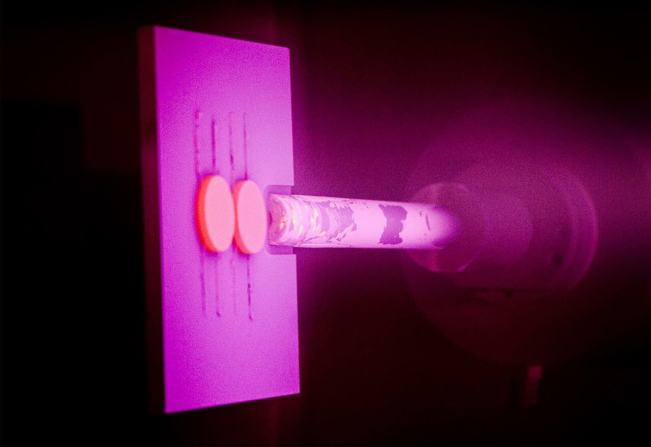
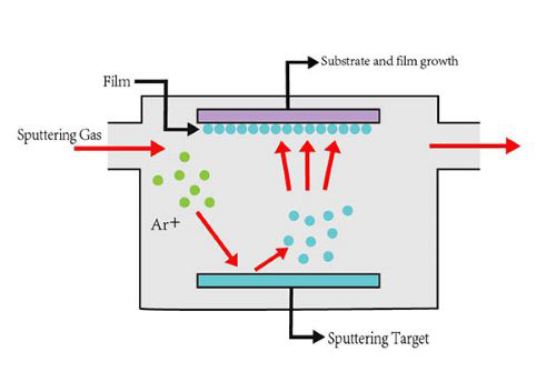
Introduction Sputtering is a cornerstone of physical vapor deposition (PVD) and stands at the forefront of materials science and advanced manufacturing. This versatile technique plays a pivotal role in the deposition of thin films onto substrates with plenty of advantages and limitations. In this article, we will delve into the world of sputtering, uncovering its...Continue Reading
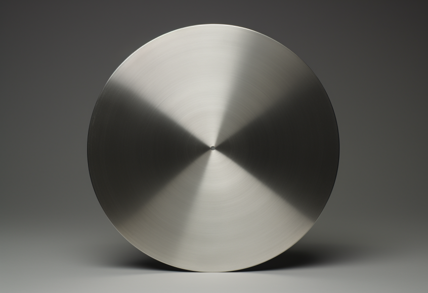
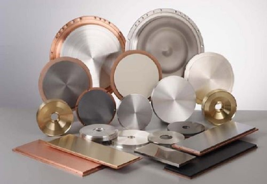
Introduction Sputtering is a common thin-film deposition technique used in various industries, including semiconductors, optics, and surface coatings. A sputtering target is a key component in the process, as it is responsible for generating the material to be deposited onto a substrate. It is important to ensure that the sputtering target is used at a...Continue Reading
Introduction The deposition rate is an important factor in the field of thin film deposition, as it directly affects the production efficiency and throughput of the process. In this article, we will discuss practical methods to increase the deposition rate for various deposition techniques. Hope that you can have a better understanding of the factors...Continue Reading