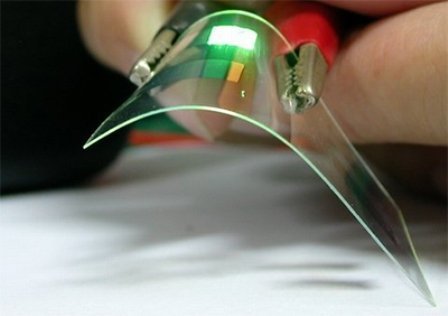
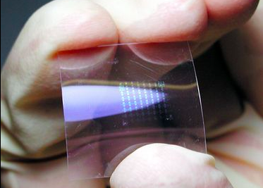
The Importance of Film Coating for Semiconductors
The Semiconductor Market: Opportunities and Threats
From both of the perspective of technology or economic development, the importance of semiconductors is enormous. Most of today’s electronic products, such as computers, mobile phones or digital recorders, have a very close relationship with semiconductors.
Along with the rapid development, the semiconductor market also faces some challenges. First, With more and more devices connecting to and thriving on the IoT (Internet of Things), the wireless connectivity and speed is a concern; Second, water-resistant or waterproof mobile devices are a huge draw for consumers; Third, devices need to be reliable and durable, withstanding constant, prolonged use and occasional rough handling. All of those are important requirements for semiconductor chips to meet and challenges for semiconductor supplier to solve.
Film Coating Solution for Semiconductors
Thin film deposition can help solve these challenges. Applying a thin film coating on the semiconductors can not only improve their efficiency, but also extend their service life. However, to acquire a good quality film, semiconductor manufacturers have to make sure that the coating materials, commonly sputtering targets or evaporation materials, are of high purity.
Improve the efficiency
Thin layers from metal elemental like copper (The link goes to the copper film coating material), aluminum, goldor silver etc. and alloys have found numerous applications in semiconductor devices. Due to their high electrical conductivity, they are able to transport electrical currents or supply voltages.
Thin metal layers serve in the conventional electrical system, for instance, as Cu layers on printed circuit boards, as the outer ground conductor in coaxial cables and various other forms like sensors etc.
Another major application of semiconductor is in integrated circuits, where the electrical network among active and passive devices like transistors and capacitors etc. is built up from thin Al or Cu layers. These layers dispose of thicknesses in the range of a few 100 nm up to a few µm, and they are often embedded into a few nm thin titanium nitride layers in order to block a chemical reaction with the surrounding dielectric like SiO2.
Waterproof
For the finished consumer product, diamond-like carbon (DLC) coatings can provide maximum protection against scratching and breaking of the components. DLC coatings should also be applied to outer displays, such as phone screens, for the same protection. To waterproof the finished products, hydrophobic coatings can be applied on either the chip or device level, providing manufacturers with multiple options to achieve water resistance, depending on the cost of production and performance goals.
Extend the service life
Most semiconductors have a natural lifespan that ends in a wear out mechanism. Defects in construction in the active area can reduce the lifetime significantly and are particularly affected by current and temperature. Although these degradation failures are unavoidable, applying a hardware thin film can prolong the lifetime of the semiconductor.
The use of the correct coating on the drive circuitry and frames can mitigate against the corrosive effects of the operating environment. This is achieved by the coating to behave as an effective barrier to extraneous contaminants, allowing for preservation of the circuit’s integrity, as well as mitigating against the potential effects of tin whiskers.
For more information about semiconductor coatings, you can contact us, and we are willing to provide solutions for your semiconductor coating project. Also, you can also visit our website https://www.sputtertargets.net/ for more information about coating materials. Feel Free to send us a price inquiry.


