How Is The Chip Made?
In modern life, people can not get away from sputtering targets at all times. Smartphones, credit cards, cameras, two generation ID cards… They all have a chip. The ultra-thin metal wire, which is nearly 10000 meters in length, is made of the sputtering target. High purity sputtering target is a key material in semiconductor chip manufacturing. The core of these metal targets is their purity. The purity of the general metal is 99.8%, while the metal purity required to make the chip is 99.999%.
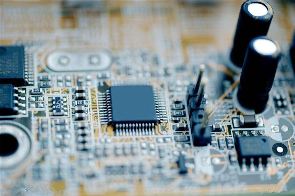
The whole process of chip fabrication includes chip design, wafer fabrication, encapsulation, and test. Wafer fabrication is particularly complicated.
First is the chip design, according to the design requirements, the “pattern” generated.
1, the raw wafer of the chip
The composition of the wafer is silicon. The wafer is purified by silicon element (99.999%). Then, some pure silicon is made into silicon crystal bar to make the quartz semiconductor of the integrated circuit. The chip is the crystal circle. The thinner the wafer is, the lower the cost of production is, but the higher the process requirement is.
2, wafer coating
Wafer coating can resist oxidation and heat, and its material is a kind of photoresist.
3, wafer lithography development, etching
The process uses chemicals, which softens when exposed to ultraviolet light. The shape of the chip can be obtained by controlling the position of the shading object. The silicon wafer is coated with a photoresist so that it will dissolve in ultraviolet light. This is the first shade that can be used to dissolve the direct part of the ultraviolet light, which is then washed away by solvent. The rest is just the same as the shape of the shading, which is exactly what we want. So we get the silicon dioxide layer we need.
4, adulterate impurities
Implantation of ions into the wafer generates corresponding P and N semiconductors.
The specific process is to start from the exposed area on the silicon wafer and put it into the chemical ion mixture. This process will change the way of conduction in the doped area, so that each transistor can pass, break, or carry data. A simple chip can be used only one layer, but the complex chip usually has many layers, and this process is repeated, and the different layers can be joined through the open window. This is similar to the principle of making the PCB board. More complex chips may require multiple silicon dioxide layers. This is achieved by repeating photolithography and the above process to form a three-dimensional structure.
5. Wafer test
After the above process, there are a lot of lattice grains on the wafer. Electrical characteristics of each grain were detected by needle testing. In general, the number of grains per chip is huge, and it is a very complicated process to organize the one needle test mode, which requires the mass production of the model of the same chip as the same size as possible in production.
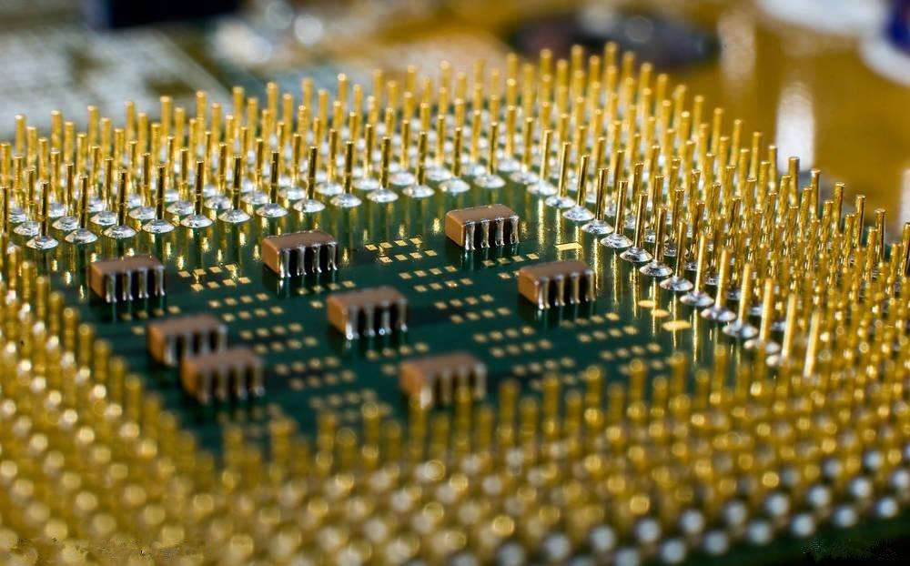
6, encapsulation
The wafer is fixed, the binding pin, according to the demand makes the different encapsulation form, this is the same chip core can have the different encapsulation form. For example: DIP, QFP, PLCC, QFN and so on. This is mainly determined by the user’s application habits, application environment, market forms and other peripheral factors.
7, test, packaging
After the above process, chip production has been completed, this step is to test chips, remove defective products, and packaging.
Stanford Advanced Materials (SAM) Corporation is a global sputtering target manufacturer established in 1994. For more information, please visit https://www.sputtertargets.net/.


