High-Purity Niobium Sputtering Targets in Semiconductor Chip Fabrication
Introduction
Thin film deposition is an integral part of semiconductor chip production. Sputtering is perhaps the most established and reliable method of placing smooth films on wafers. Among all the materials that have been employed as targets, niobium stands out for its unique combination of electrical, thermal, and chemical properties that qualify it perfectly for a wide range of semiconductor applications.
Niobium sputtering targets are critical components not only used as plain conductive layers but also play a vital role in superconducting film and diffusion barrier formation in complex chips. Their performance directly affects the reliability and effectiveness of devices.
Material Characteristics
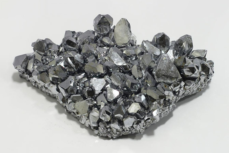
Niobium has a melting point of around 2,477°C and is also resistant to most corrosive chemicals with good electrical conductivity. For semiconductor use, the Niobium targets are produced with purities of 99.995% or higher. This prevents unwanted contaminants from penetrating the deposited layer, satisfying chipmakers’ very stringent levels of contamination.
Film performance is also a function of the internal structure of the target. Fine, homogeneous grains allow for uniform erosion during sputtering and yield more consistent layer thickness in wafers. Due to its mechanical strength, niobium can be produced in large-diameter targets suitable for current high-volume tools.
Production Process
Production of a high-purity niobium target involves several main steps:
-
Powder purification – Advanced refining removes metallic and non-metallic impurities before consolidation.
-
Melting and consolidation – Vacuum melting or electron beam melting produces a homogeneous ingot, which is then densified using hot isostatic pressing (HIP).
-
Grain and texture control – Thermal treatments help set the right microstructure for steady sputtering performance.
-
Precision shaping – Machining to exact tolerances ensures good fit in deposition systems and uniform erosion patterns.
-
Final inspection – Purity levels, density, grain size, and bonding compatibility are all verified before shipment.
Applications in Semiconductor Chip Fabrication
Thin film deposition
Niobium targets are widely utilized in DC magnetron sputtering equipment. Engineers rely on them to deposit conductive films or diffusion barriers of controlled thickness. For instance, a 50–100 nm layer of niobium can be employed as a barrier between silicon substrates and copper interconnects.
Formation of conductive layers and diffusion barriers
Superconducting films for advanced devices
Certain semiconductor chips, including quantum processors and sensitive detectors, require superconducting thin films. Niobium deposited under controlled conditions maintains cryogenically stable superconductivity, supporting low-loss signal routes and high device performance.
Device-Level Applications
Transistors, capacitors, and interconnects
Niobium films improve conductivity and thermal stability in dense circuits. Uniformity in such films provides consistent electrical behavior, which reduces resistive losses in high-frequency applications.
Protective and barrier layers
In multilayer devices, niobium serves as a metal migration or chemical contamination barrier. It shields the semiconductor from potential defects in future processing.
Specialized superconducting chips
When chips will be operated at cryogenic temperatures, the superconducting characteristic of niobium becomes essential. Niobium can be deposited to allow engineers to fabricate Josephson junctions or other superconducting devices with high precision and low defects.
Micro- and nanoelectronics integration
The precision of niobium sputtering allows for nanoscale production. Films with the minimum thickness of a few nanometers can be deposited with high uniformity, which is needed in modern nanoelectronics and test devices.
Conclusion
Niobium sputtering targets play an operational, process-related role in the production of semiconductor chips. Their durability under extreme deposition conditions, together with their success as barrier and conducting films, renders them a solid material for advanced device manufacturing. With chips still growing in complexity, the application of niobium in PVD processes must also remain topmost on the agenda for guaranteeing performance and reliability.
Visit Stanford Advanced Materials’ homepage to see more sputtering target products.


