Copper Sputter Targets: Shapes and Applications
Copper sputter targets are used to deposit thin metal films on various substrates. They are chosen for their electrical and thermal conductivity, ductility, and adhesion properties. Thin films from copper appear in electronics, solar cells, displays, and decorative coatings. The shape and size of the target influence deposition uniformity and material usage.
Target Shapes
Planar Targets
Planar targets are flat and sit parallel to the substrate. They include square, disc, and plate shapes.
-
Square targets are compact and wear evenly. Typical sizes range from 50 mm to 150 mm per side, with thickness between 5 mm and 15 mm. They are easy to mount and replace in small chambers or pilot setups.
-
Disc targets are circular. Diameters usually range from 50 mm to 200 mm, with thicknesses from 5 mm to 20 mm. They rotate or remain stationary depending on the system, providing uniform material distribution. Magnetron sputtering often uses these targets for sensors and microelectronic devices.
-
Plate targets are thicker, typically 5–25 mm. They provide more material for longer runs. Custom sizes can match specific chamber shapes or experimental setups.
Rotary Targets
Rotary targets turn during sputtering, which improves material use and ensures even deposition.
-
Cylindrical targets are used in large displays and decorative coatings. Diameters range from 50 mm to 300 mm, with lengths up to 1500 mm. Internal magnets help stabilize sputtering and reduce edge erosion.
-
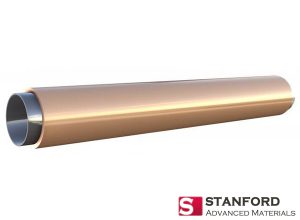
Tube targets are hollow and machined precisely. They usually have wall thicknesses of 3–10 mm, diameters of 50–150 mm, and lengths up to 2000 mm. They are applied in optical coatings and industrial PVD systems where flatness and geometry control are important.
Applications
Semiconductors
Copper films carry current in integrated circuits. They form wiring, vias, and contact layers. Even at nanoscale thickness, copper maintains conductivity and structure.
Solar Cells
In CIGS thin-film solar cells, copper forms part of the absorber layer and back contact. Films adhere to the substrate and survive high-temperature processes. In CdTe cells, copper can be used for back contacts or doping. Engineers monitor film thickness to control efficiency and reliability.
Flat Panel Displays
Copper is applied as electrodes and interconnects in LCD and OLED panels. Smooth surfaces and low resistance improve image quality. Uniform deposition prevents pixel defects and ensures display stability.
Decorative Coatings
Copper coatings provide shine and corrosion resistance. Applications include automotive trim, architectural accents, and consumer electronics. Thin copper layers protect underlying metals while retaining a metallic appearance.
Optical Coatings
Copper reflects visible and infrared light. It is used in mirrors, filters, and IR sensors. Layer thickness and uniformity affect reflectivity and thermal performance.
Notes on Target Selection
- Purity: Targets with 99.95% or higher copper are common for electronics.
- Dimensions: Thickness, diameter, and shape must fit the sputtering chamber.
- Surface Finish: Smooth, defect-free surfaces improve deposition uniformity.
- Wear Monitoring: Erosion patterns and deposition rate are checked during runs.
SAM Supply
Stanford Advanced Materials (SAM) supplies copper targets in square, disc, plate, cylindrical, and tube forms. Targets are machined for flatness and uniform thickness. Custom orders, tight tolerances, and batch consistency support lab and production environments.


