Gold Sputter Target for LED Lighting Application
Gold Sputter Target Demand Increases As LED Market Grows
The LED industry has grown rapidly over the past decade partially due to the penetration of LED-backlit TVs and laptops. One of the most important functional components of the LED is the LED semiconductor chip. At present, the materials used in the manufacturing of LED chips are mainly gold sputter target and gold evaporation material.
LED lights outperformed incandescent lamps in energy efficiency and longevity, which has been the major reason for the growth of the LED lighting market. LED lighting systems have been used in emergency, backlight, automotive, indoor and outdoor applications. Gold sputtering targets and gold evaporation materials are extensively used for thin film deposition, a core technology used in the manufacturing of LED chips. The price of gold has continued to increase in the last few years and the trend is expected to continue. (If you would like to acquire more information about the sputtering target price, please send us an inquiry)
Gold Sputter Target for LED Chips
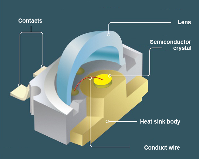
The most fundamental and crucial component of the LED light is the LED chip, also known as the semiconductor crystal. The chips are very small- standard measurements are 10×16, 10×23, or 45×45 mils (thousandths of an inch) – to see a single chip clearly, a microscope is needed. The LED chip is where all the action happens – it is the diode itself (as in Light Emitting Diode), and is oftentimes the most cost-intensive component in LED product manufacturing.
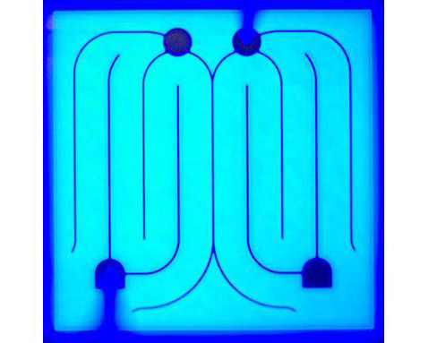
High-purity gold sputter target has excellent physical and chemical properties, such as low contact resistance and stability, easy bonding, and easy film formation. By adding other elements, gold can be alloyed to Gold Germanium, Gold Gallium, and Gold Beryllium. The flow point of these materials can be changed, and their wettability and adhesion with different materials can also be improved. What’s more, they can form an ohmic contact with the compound semiconductor, thus are the key base materials for semiconductor manufacturing. They use different kinds of gold-based sputtering and evaporation materials, including Au/GaP, Au/AuBe/GaP, AuGeNi/GaAsP, Au/GaAs, AuGeNi/Au/GaAs and Au/GaN in the thin film deposition process.
Manufacturing Process of LED chips
One of the reasons why LED chips comprise a significant portion of the total cost in producing an LED product is due to its extremely high-precision manufacturing process. The basic manufacturing Process of LED Chip is shown below.
Epitaxial wafer → cleaning → plating transparent electrode layer → transparent electrode pattern lithography → corrosion → debonding → platform pattern lithography → dry etching → debonding → annealing → SiO2 deposition → window pattern lithography → SiO2 etching → deagglomerating → N-pole pattern lithography → pre-cleaning → coating → stripping → annealing → P-pole pattern lithography → coating → stripping → grinding → cutting → chip → finished product testing.
Choose SAM’s Gold Sputter Target
Thanks for reading this passage and hope that you now have a basic understanding of titanium dioxide film. Stanford Advanced Materials (SAM) is a leading sputtering target manufacturer based in Lake Forest, California. SAM provides a one-stop solution from manufacturing gold sputter targets, to meeting precise standards for excellent thin film properties and high yields, to bonding strong backplate, to reclaiming precious metals and then refining reclaimed metal back to its original specifications, and to fabricating it again into usable thin film deposition material. If you feel interested about the gold sputter target, you can go to our product page for more information, or directly send us an inquiry. You can also contact us via target@samaterials.com. Free samples are available.


