Indium Tin Oxide in Chemistry
When it comes to the abbreviation “ITO”, it can stand for International Trade Organization, Involuntary Treatment Order, or Information Technology Outsourcing. But in chemistry, “ITO” refers directly to a crucial chemical material — Indium Tin Oxide.
What is Indium Tin Oxide in Chemistry?
Indium tin oxide (ITO) is a black-gray ceramic material composed of indium oxide and tin oxide in a certain ratio. Renowned for its excellent electrical conductivity and transparency, ITO also possesses the ability to block electron radiation, ultraviolet rays, and far-infrared rays, which are harmful to the human body. As such, ITO films are typically sprayed onto glass, plastic, and electronic display screens, used as a transparent conductive film that simultaneously reduces harmful electronic radiation across ultraviolet and infrared spectrums. The ITO sputtering target is an essential material for producing these ITO films.
Broad Applications of ITO
Indium Tin Oxide is integral to several modern technologies, especially in devices where transparency and conductivity are essential:
- Touch Screens: ITO’s exceptional conductivity and transparency are crucial in smartphones, tablets, and interactive kiosks, ensuring accurate touch responsiveness and clear display.
- Flat Panel Displays: Used in LCDs and OLEDs, ITO contributes to high-quality, energy-efficient displays with excellent color fidelity.
- Solar Cells: ITO’s application in solar panels enhances their efficiency; its transparency allows light to penetrate while its conductivity facilitates electron collection for electricity generation.
Detailed Properties of Indium Tin Oxide
The physical and chemical properties of ITO are key to its versatility in various applications:
| Property | Value | Reference |
| Mass density | 6.8 g/cm3 | J Vac Sci Tech A 19:5(2043-7); 2001 |
| Young’s modulus (sputtered, 10wt% SnO2) | 116 GPa | Thin Solid Films 278:1-2(12-17); 1995 |
| Poisson ratio (sputtered, 10wt% SnO2) | 0.35 | Thin Solid Films 278:1-2(12-17); 1995 |
| Tensile or fracture strength failure strain (105 nm film) failure strain (16.8 nm film) |
0.022 0.003 |
MRS Symp Proc 666 (F3.24.1 – 12); 2001 |
| Residual stress on silicon (sputtered, 10wt% SnO2) |
-2.1 ~ -2.3 GPa | Thin Solid Films 278:1-2(12-17); 1995 |
| Index of refraction (increases with annealing) |
~1.7 @633 nm 1.8 – 2.0 |
Appl Surf Sci 179:1-4(181-90); 2001 J Vac Sci Tech A 19:5(2514-21); 2001 |
| Electrical conductivity (“standard” sputtered) (epi, 5.7wt% SnO2) |
~104 S/cm 1.3 x 10⁴ S/cm |
Thin Solid Films 411:1(1-5); 2002 Vacuum 66:3-4(419-25); 2002 |
| Piezoresistivity: gage factor (sputtered) (laser deposited) |
0.2 ~ -14.7 2.04 ~ -77.71 |
J Appl Phys 91:9(6194-6); 2002 Thin Solid Films 288 (279-286); 1996 |
| Wet etching method | oxalic acid HCl/HNO3 |
Langmuir 18:1(194-7); 2002 J Electron Mat 25:12(1806-17); 1996 |
| Plasma etching method | CH4/H2/Ar | J Vac Sci Tech A 16:4(2177-86); 1998 |
| Adhesion to silicon dioxide | good – in pull off tests of 1000 Å ITO and 1300-30,000 Å SiO2, failures occurred in substrate rather than ITO/oxide. | Appl Surf Sci 115:1(96-102); 1997 |
| Biocompatibility | no observed inhibition of cell growth; a small amount of protein adsorption | Proc IEEE/EMBS Conf on Microtechnologies in Medicine & Biology (261-4);2002 |
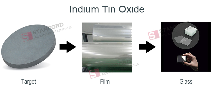
Indium Tin Oxide Derivatives
Various derivatives of indium tin oxide, such as ITO sputtering target, ITO film, and ITO glass, are crucial in different applications. Below are their detailed properties and uses.
1. Indium Tin Oxide Sputtering Target
Indium tin oxide sputtering target (ITO sputter target) is a mixture of indium trioxide (In2O3) and tin dioxide (SnO2), and is an important raw material for the preparation of ITO films. The theoretical density of the ITO target is 7115 g/cm3, while the high-quality ITO target should have a relative density of ≥99%. Such ITO targets have lower electrical resistivity, higher thermal conductivity, and higher mechanical strength. The high-density target can be sputtered on a glass substrate at a lower temperature to obtain a conductive film having lower resistivity and higher light transmittance and even can be sputtered on the organic material.
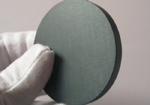
There are four main ways to mold ITO sputtering targets, including spraying, cold isostatic pressing, hot isostatic pressing, and wet forming. You can refer to Everything You Need to Know About ITO Sputtering Target for more information.
2. Indium Tin Oxide Film
Indium tin oxide film (ITO film) is an ITO semiconductor transparent conductive film prepared by vacuum evaporation or sputtering deposition. The film has high conductivity, high visible light transmittance, high mechanical hardness, and good chemical stability.
In recent years, ITO film has become more and more advantageous in the film manufacturing industry and has become one of the best-performing transparent conductive oxides (TOCs). It is also the most commonly used thin-film material for transparent electrodes of liquid crystal displays (LCDs), plasma displays (PDPs), electroluminescent displays (EL/OLEDs), touch panels (TouchPanel), solar cells, and other electronic meters.
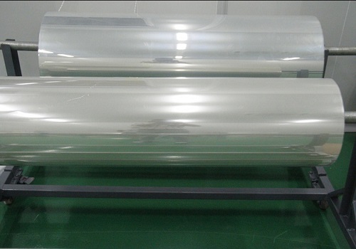
The transmittance and resistance of the ITO film are controlled by the ratio of In2O3 and SnO2, respectively. Increasing the ratio of indium oxide can increase the transmittance of ITO, usually SnO2: In2O3=1:9. Since the thickness of tin oxide exceeds a certain degree, the transparency is usually not good enough – although the conductivity is good.
3. Indium Tin Oxide Glass
Indium tin oxide conductive glass (ITO glass) is made by processing a layer of ITO film by sputtering, evaporation, etc. based on soda-lime-based or silicon-boron-based glass. Most electronic displays are ITO glasses.
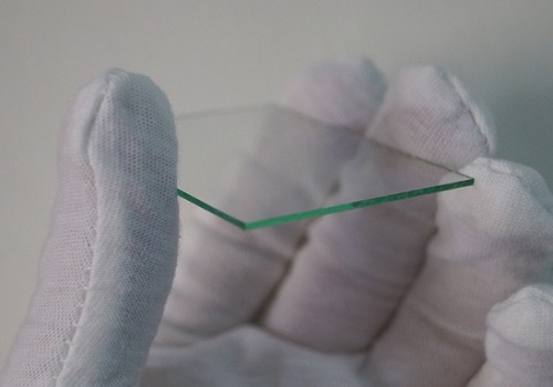
The ITO conductive glass applied to the LEDs also needs to be coated with a silicon dioxide barrier layer before the ITO layer is plated to prevent sodium ions on the substrate glass from diffusing into the liquid crystal in the cell. The ITO glass substrates for LEDs are generally ultra-float glass, and all the coated surfaces are glass float tin surfaces. Therefore, the final LEDs will follow the direction of the float, and irregular ripples will occur regularly.
Conclusion
Indium Tin Oxide’s unique properties make it indispensable in consumer electronics and renewable energy fields. Its ability to combine transparency with conductivity while blocking harmful radiation allows for innovative applications in cutting-edge technologies. For further information or inquiries about ITO sputtering targets and other products, Stanford Advanced Materials (SAM) at target@samaterials.com. Free samples are available upon request.
Send Us An Inquiry Via Online Form


