Everything You Need to Know About Sputtering Targets
1. Introduction to Sputtering Targets
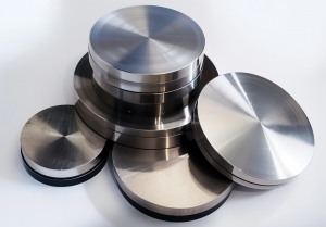
Sputtering targets are significant commodities for thin-film industries like electronics, optics, and energy sectors. Simply put, a “sputtering target” is the target material utilized for sputtering, a form of physical vapor deposition (PVD). During the PVD process, atoms from a solid target are removed and ejected upon impact by high-energy ions hitting the target surface. These atoms are deposited on a substrate and develop into thin films. The process is critical for the manufacture of thin films, which are paramount elements for contemporary devices—from semiconductors and optical coatings to solar panels.
As the requirements for the devices become more stringent, sputtering targets are evolving to provide higher purity and tailored compositions for particular applications. Some applications now make use of tailored alloy or ceramic targets for particular desired electrical, optical, or magnetic properties.
2. Composition and Types of Sputtering Targets
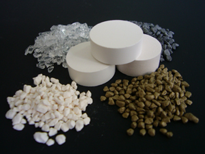
Sputtering targets are produced from an array of materials, chosen considering the utilization purpose and the desired thin-film quality. Material selection directly affects the quality and the performance of the final product. The following are the main types of sputtering targets used industrially.
2.1 Metal Targets
Metal targets are suitable for applications that require conductive films, such as semiconductor devices and electrical components.
- Pure Metal Targets: Aluminum (Al), copper (Cu), nickel (Ni), gold (Au), and silver (Ag) are common metals. High-purity grades are typically required to minimize contamination in sensitive applications.
- Alloy Targets: Alloys combine two or more metals to achieve specific properties. For example, Titanium-tungsten (TiW) alloy targets are widely used in semiconductor fabrication for metal interconnect layers because they offer both high conductivity and good adhesion.
2.2 Ceramic Targets
Ceramic materials boast durability, chemical stability, and resistance to heat and wear. Most ceramic targets are non-conductive, making them ideal for optical coatings and protective layers.
- Oxide Targets: Aluminum oxide (Al2O3) and titanium dioxide (TiO2) are common oxides. They are used for corrosion-resistant coatings in optical lenses and display screens.
- Nitride Targets: Aluminum nitride (AlN) and silicon nitride (Si3N4) provide excellent thermal conductivity and electrical insulation. They are suitable for high-temperature electronics and aerospace components.
- Carbide Targets: Silicon carbide (SiC) and tungsten carbide (WC) are extremely hard and wear-resistant, making them suitable for protective coatings in cutting tools and automotive parts.
2.3 Compound Targets
In addition to metals and ceramics, compound materials are used in sputtering targets to achieve specific thin-film properties:
- Silicide Targets: These materials offer excellent electrical conductivity. For example, Titanium silicide (TiSi₂) and tungsten silicide (WSi₂) are critical in semiconductor manufacturing.
- Fluoride Targets: These targets are essential in producing optical devices like lenses and coatings for lasers. Calcium fluoride (CaF₂) and magnesium fluoride (MgF₂) are used in optical coatings for their high transparency in the UV and infrared spectra.
- Sulfide Targets: Zinc sulfide (ZnS) and molybdenum disulfide (MoS₂) are used in thin films for photovoltaic cells and lubricating coatings. ZnS is also a key material in optical and display applications due to its transparency.
- Boride Targets: Silicon boride (BSi) and titanium boride (TiB₂) are known for their high hardness and thermal stability. They are commonly used in high-temperature applications and semiconductor industries where durable coatings are needed.
- Selenide Targets: Copper indium gallium selenide (CIGS) and zinc selenide (ZnSe) are widely used in solar cells and infrared optical devices. CIGS targets are crucial for high-efficiency thin-film solar panels, while ZnSe is used in lenses and windows for infrared applications.
- Telluride Targets: Telluride compounds like cadmium telluride (CdTe) and bismuth telluride (Bi₂Te₃) are extensively used in thermoelectric devices and photovoltaic cells. CdTe is a significant material in solar panels, while Bi₂Te₃ is used for energy harvesting in thermoelectric generators.
- Rare Earth Targets: Rare earth elements, such as gadolinium (Gd), neodymium (Nd), and yttrium (Y), are used in sputtering targets for applications requiring magnetic, luminescent, and catalytic properties. These materials are critical in producing advanced magnets, lighting technologies, and high-performance coatings.
2.4 Functional and Application-Specific Targets
Some other targets are categorized by their functions or the applications they are used in, rather than their chemical composition:
- Magnetic Materials: Iron (Fe) and nickel-iron (NiFe) targets create magnetic layers in data storage devices.
- Semiconductor Targets: Silicon (Si) and germanium (Ge) enable thin films for integrated circuits and infrared sensors.
- Composite Targets: Combining metals and ceramics allows coatings that are both conductive and wear-resistant. They are useful for protective layers in electronics and precision components.
3. Manufacturing Process of Sputtering Targets
3.1 Manufacturing Techniques
There exist numerous sputtering target manufacturing methods. As the material and level of target performance desired, the method employed can differ.
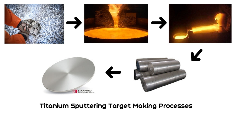
- Melting and Casting: Metal targets use this method the most. Raw metals are melted in a vacuum or controlled atmosphere to prevent contamination, then cast into molds of the desired shape. Vacuum or inert-atmosphere casting helps achieve high purity and low porosity. These qualities are important for uniform sputtering and high-quality thin films. Commonly, aluminum and copper targets for semiconductor interconnect layers are produced this way.
- Sintering: Powdered materials are compacted and heated below their melting point to form solid targets. This method is often used for ceramic and compound targets, such as oxides, nitrides, and carbides. This process allows precise control of density, grain structure, and porosity, which are critical for consistent film deposition.
- Hot Isostatic Pressing (HIP): HIP increases density by applying high temperature and pressure simultaneously. This technique is especially useful for ceramic or composite targets that require low porosity and high mechanical strength. HIP is also commonly applied to high-purity metal targets to improve uniformity and reduce defects.
- Cold Isostatic Pressing (CIP): Conducted at room temperature, CIP is mainly used to form high-density preforms from powders before sintering or HIP. It ensures uniform compaction and improves the final target’s properties, particularly for ceramics and composites.
3.2 Process Workflow
The typical manufacturing process for sputtering targets involves some basic steps, and all of them affect the end product performance:
-
Material Preparation: Raw materials are selected based on purity and composition. For metal targets, this involves melting and alloying. Ceramic and compound targets are prepared as powders through grinding, mixing, and sometimes calcination or ball milling. High-purity materials help ensure consistent thin-film deposition.
-
Shaping: Targets are formed according to material type and required geometry. Metal targets are typically cast into molds, while ceramic and composite materials are compacted using pressing or extrusion techniques. The shaping step influences density, grain structure, and uniformity.
-
Sintering and Pressing: Powdered materials are sintered to consolidate particles into a dense solid target. Hot isostatic pressing (HIP) can further increase density, reduce voids, and improve mechanical strength. These steps are especially important for high-purity metals and composite or ceramic targets.
-
Machining and Surface Treatment: After forming, targets are machined to precise dimensions using lathes, grinders, or milling machines. Surface treatments, including polishing or specialized coatings, enhance sputtering performance and film uniformity. Advanced processes may also control surface roughness to meet high-end semiconductor or optical requirements.
-
Quality Control: Each target is tested to verify purity, density, and surface quality. Common methods include X-ray fluorescence (XRF), inductively coupled plasma (ICP) analysis, and optical microscopy. Additional inspections, such as ultrasonic testing or 3D surface profiling, are increasingly used to meet modern high-performance standards.
3.3 Control of Grain Structure
Target sputtering performance is an essential feature of the grain structure. Grain orientation and size can affect the quality of thin-film uniformity and the sputtering material’s deposition rate. Smaller grains are desirable for maintaining stable deposition rates because they tend to eject the material more uniformly throughout the sputtering process. Furthermore, the ability to control the orientation of grains—best suited for equiaxed grains (where the grains are roughly the same size and shape in all directions)—enhances the sputtering process stability and minimizes the inconsistency of the thickness within the films.
To restrict the grain direction, the manufacturers apply sophisticated process methods like:
- Powder metallurgy for producing fine-grain ceramics and composites.
- Controlled cooling rates during casting or sintering to influence the final grain size.
- Post-processing treatments like annealing which can refine the grain structure and enhance material properties.
4. Applications of Sputtering Targets
4.1 Semiconductor Manufacturing
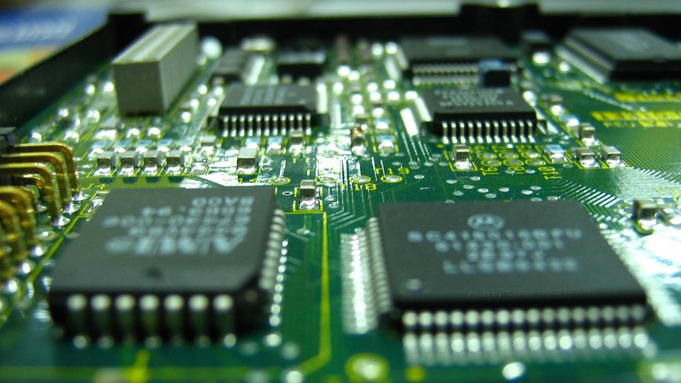
Sputtering deposits thin layers of metals and dielectric materials on silicon wafers. They make up the primary elements of integrated circuits and electronic devices used for the fabrication of semiconductor industry products. For example, aluminum is normally utilized for metal interconnect layers since it possesses very good conductance, thus allowing for good electrical contacts. Titanium and titanium-tungsten (TiW) alloy layers are typically utilized as a barrier/adhesion layer between the metal interconnect and the silicon, preventing diffusion and showing stable electrical performance.
4.2 Data Storage (Hard Drive Manufacturing)
The information storage sector employs sputtering for the manufacture of hard drives and other storage device magnetic thin films. High-density storage and stable coercivity are employed for the Co-base alloy, such as CoCrPt or CoPtCrSiO₂, for the purpose of the magnetic layers. Materials are designed for improved corrosion resistance and stable data durability for the long term.
4.3 Optical Devices
Anti-reflecting coatings of silicon dioxide (SiO₂) are normally used for light reflectance minimization and attainment of maximum clarity for cameras, microscopy, and highly accurate measuring tools. For instance, Indium tin oxide (ITO) permits the manufacturing of clear conductive films for LCD and touchscreen applications. Some of the additional modern-day applications include protective coatings for UV and infrared (IR) applications for increased quality optical systems.

4.4 Solar Cells
Aluminum-molybdenum (Al-Mo) alloy back electrodes provide high conductivity, permanent adhesion, and enhanced corrosion resistance. And copper indium gallium selenide (CIGS) targets form absorbers that convert solar photons into electrical current. Higher-order technologies generally use perovskite or multi-layers for enhanced conversion efficiency.
4.5 Protective and Decorative Coatings
Sputtering yields hard and decorative metal, glass, and ceramic coatings. For example, titanium nitride (TiN) provides gold-appearing, wear-resistant coatings for watches, jewelry, and high-end tools, equating appearance with hardness and resistance to corrosion. Chromium coatings protect metal and glass surfaces for auto or building uses. Other modern coatings include aluminum titanium nitride (AlTiN) and diamond-like carbon (DLC), which offer higher wear resistance and hardness for cutting tools and precision parts.
5. Factors to Consider When Choosing Sputtering Targets
The quality of your thin films will be determined by your choice of sputtering target. Uniformity, adhesion, and thickness are all regulated by the target. Below are the most critical factors to bear in mind before you make your choice.
5.1 Why Purity Is Important
Thin-film coatings live or die depending on purity. A trace of oxygen or water in the target will shatter adhesion or create weak points that will peel out later. Trace contamination in semiconductors will break up conductivity. Copper is one example: the higher the sulfur content, the more you can count on micro-cracks or electrical discharge. That is why most critical industries now expect purities of 99.995% and higher, especially for optics, interconnects, and magnetic films.
5.2 Film Density and Uniformity
Dense targets make smooth, uniform films. Porous targets don’t. The oxygen is trapped in the pores, released during sputtering, and the film is cracked or irregular. Semiconductor and optical makers generally want densities of more than 98%. In powder metallurgy, 97% and above is norm, often with HIP or CIP to push out the last shred of porosity and keep sputtering in line with heat and pressure.
5.3 Grain Size and Deposition Rate
Grain size controls the rate and uniformity with which a target erodes. Fine grains sputter at a steady rate and deposit material more uniformly over the substrate. Coarse grains deposit thickness irregularities and patches. Ultra-fine grain can be produced using processes like ball milling followed by HIP or CIP, the choice for electronics and optics of high precision.
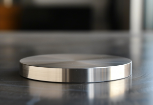
5.4 Shape and Material Use
Target geometry is not really about fitting into the system—it decides how much material you can actually handle. Planar, flat targets are okay with small substrates when you need surface homogeneity. Rotating cylinders are better with big panels. They last longer, consume less material, and keep the coating even. Some designs even use composite or layered targets to trade conductivity for wear resistance, especially in displays and more advanced chips.
5.5 Homogeneity of the Target
And it’s not only purity and density—homogeneity throughout the whole target is just as significant. Any compositional or structural variation can express itself as non-uniform film thickness or erratic electrical behavior. Smooth surfaces and oriented crystal control are also sought after for high-performance applications to ensure device predictability.
5.6 How Processing Influences Performance
How it’s built is as important as what it’s built with. Voids are eliminated and density is raised by high-temperature pressing or HIP. CIP helps shape and pre-densify powders before sintering. Cooling rate changes the grain structure, and the structure controls how the target sputters. Further treatments like annealing or polishing can stabilize the surface and improve manufacturing repeatability.
6. Maintenance and Handling
Targets not just need to be made right, they need to be handled, stored, and monitored right. A careless hand or humid warehouse can undo the attention taken to make them.
6.1 Storage
Keep targets clean, dry, and stable. Storage in a cleanroom is optimal for semiconductor and optical materials. Avoid temperature or humidity oscillations; metals like copper and aluminum corrode quickly under these conditions. Vacuum-sealed pouches or nitrogen purge are common methods to protect reactive surfaces.
6.2 Handling
Always use lint-free gloves and precise tools. One fingerprint will ruin adhesion on the next film run. Don’t touch the sputtering surface, and don’t force brittle ceramics into place. Use good mounting hardware and be patient—it saves both the target and coating quality.
6.3 Inspection and Cleaning
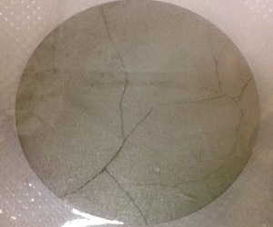
Check targets regularly. Look for cracks, chips, or extensive erosion. Replace them before they start eating away at the coating. For oxidizable metals like copper, clean carefully with qualified solvents (or ultrasonic cleaning for delicate parts) to maintain surface quality. Keep an eye on erosion rates so that you know when a target is reaching the end of its useful life.
6.4 Transport
Targets are fragile, especially ceramic ones. They need real protection for shipping. Foam inserts, vacuum seals, clear “fragile” stickers, and low-vibration shipping boxes all serve to lower the risk of breakage. One shock during shipping can lead to a batch failure later.
7. Conclusion
Above all, targets are essential to thin film deposition, and thin films are the backbone of many high-technology industries, including semiconductors, data storage, optics, solar and decorative coatings. Film uniformity, adhesion, and functional performance are all directly affected by target material choice and manufacturing process and handling process.
Critical parameters such as target purity, density, grain structure, and surface finish must be thoroughly evaluated to meet the needs of each use. Sophisticated quality control methods such as X-ray fluorescence (XRF), inductively coupled plasma (ICP) analysis, and non-contact scanning of the surface help detect impurities, verify dimensions, and offer a flawless, smooth surface. Storage, handling, and servicing are also important to prevent contamination, oxidation, or mechanical stress, thereby ensuring uniform performance and extended target life.
Stanford Advanced Materials (SAM) offers a wide range of premium quality sputtering targets in metal, ceramics, and compound targets for special applications. Whether you are thin-film depositing to manufacture innovative semiconductors, high-efficiency solar cells, or precision optical coatings, SAM solutions are designed for even depositing, high material purity, and full utilization.
Send An Inquiry


