Sputtering Target-Potential Material King
In every era, some materials have followed the mainstream trend to become the best in the industry. In the past two years, the basic metal took off from the real estate. The new energy vehicles led the lithium, cobalt and other small metals. In the present situation, the development of the chip industry as the high technology commanding point has important strategic significance. The unstable international situation, is more like a powerful catalyst, as a sputtering target for the manufacture of necessary raw materials for a large scale integrated circuit, and may be a representative of the rising material under this mainstream trend.
What is the sputtering target?
In the semiconductor chip industry, as a high-tech high technology, the sputtering target is the necessary raw material for VLSI manufacturing. Ultra large scale integrated circuits (VLSI) are integrated circuits on a chip with more than 100 thousand components or more than ten thousand gate integrated circuits. Using this technology, an electronic subsystem and even the whole electronic system can be integrated on a chip to complete the functions of information acquisition, processing, storage and so on.
In the manufacturing process of VLSI, the sputtering technology, which belongs to the physical vapor deposition (PVD) technology, is one of the main technologies for the preparation of the electronic film materials.
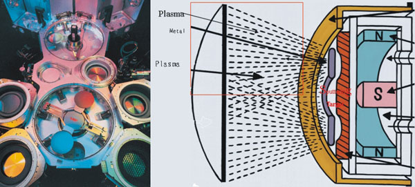
The sputtering technology uses ions produced by the ion source to accelerate the integration of high speed ion flow in the vacuum, bombardment of the solid surface, and exchange the kinetic energy between the atoms of the ions and the solid surface, and make the atoms on the solid surface leave the target and deposited on the substrate surface, thus forming nano/micron thin films.
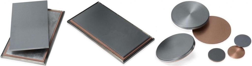
The bombarded solid is a sputtering target, which is simply a printing mold, and the quality of the target plays a vital role in the performance of the film, which directly determines the quality and performance of the downstream semiconductor chips, flat panel displays, solar cells and other electronic devices or optical components. The target material is the key raw material in the whole link.
Stanford Advanced Materials (SAM) corporation is a global sputtering target manufacturer established in 1994. For more information, please visit https://www.sputtertargets.net/.


