Detailed Introduction to Three Generations of Semiconductor Materials
What are the Three Generations of Semiconductor Materials?
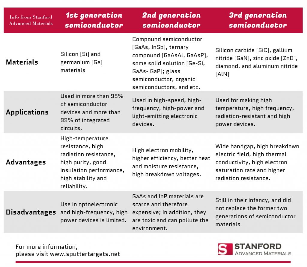
The first generation of semiconductor material
The first generation of semiconductor materials mainly refers to silicon (Si) and germanium (Ge) materials. In the 1950s, Ge dominated the semiconductor market and was mainly used in low-voltage, low-frequency, medium-power transistors and photodetectors. However, Ge semiconductor devices were inferior in high temperature and radiation resistance, and were gradually replaced in the late 1960s by Silicon devices. The semiconductor device made of silicon material has high-temperature resistance and radiation resistance. The sputtered silicon dioxide (SiO2) film has high purity and good insulation performance, which greatly improves the stability and reliability of the device. Therefore, Silicon has become the most widely used semiconductor material in that more than 95% of semiconductor devices and more than 99% of integrated circuits are made of silicon materials.
In the 21st century, its leading and core position in the semiconductor industry will remain unwavering. However, the physical properties of silicon materials limit their use in optoelectronic and high-frequency, high-power devices.
Further Reading: P-type & N-type Silicon Semiconductors
The second generation of semiconductor material
The second generation of semiconductor materials mainly refers to
1) compound semiconductor materials such as gallium arsenide (GaAs), indium antimonide (InSb);
2) ternary compound semiconductors such as GaAsAl, GaAsP, and
3) some solid solution semiconductors such as Ge-Si, GaAs-GaP;
4) glass semiconductor (also known as amorphous semiconductor), such as amorphous silicon, glass-state oxide semiconductor;
5) organic semiconductors, such as phthalocyanine, copper phthalocyanine, polyacrylonitrile, etc.
They are mainly used in the production of high-speed, high-frequency, high-power, and light-emitting electronic devices. They are excellent materials for making high-performance microwave, millimeter wave devices, and light-emitting devices. Due to the rise of information technology and the Internet, they are also widely used in satellite communications, mobile communications, optical communications, and GPS navigation.
However, GaAs and InP materials are scarce and therefore expensive. In addition, they are toxic and can pollute the environment. These shortcomings make the application of the second-generation semiconductor materials have great limitations.
The third generation of semiconductor material
The third generation of semiconductor materials is those materials with a wide bandgap (Eg≥2.3eV), represented by silicon carbide (SiC), gallium nitride (GaN), zinc oxide (ZnO), diamond, and aluminum nitride (AlN). In terms of applications, the main applications of the third generation of semiconductor materials are semiconductor lighting, power electronics, lasers and detectors, and other fields, each with different industry maturity.
Compared with the first and the second generation semiconductor materials, the third generation semiconductor materials have a wide band gap, high breakdown electric field, high thermal conductivity, high electron saturation rate, and higher radiation resistance. Therefore, it is more suitable for making high-temperature, high-frequency, radiation-resistant, and high-power devices.
Further Reading: Typical Materials of the Third Generation Semiconductors
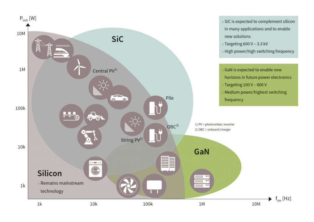
Comparison of Three Generations of Semiconductor Materials
Development Outlook of Three Generations of Semiconductor Materials
Although we have now developed into the third-generation semiconductor materials, the first and second generation semiconductor materials have not been eliminated and are still widely used. Why did the emergence of the second generation not replace the first generation? Can third-generation semiconductors completely replace traditional semiconductor materials?
Silicon and compound semiconductors are two complementary materials. In the application of semiconductors, the two are often combined to take advantage of each other, so as to produce products that meet higher requirements, such as high-reliability, high-speed products. Therefore, the first and second generation semiconductor materials are in a state of long-term commonality.
However, the third generation of wide bandgap semiconductor materials has many excellent properties, which can break through the development bottleneck of the first and the second generation semiconductor materials. With the development of technology, the third generation is expected to completely replace the first and second generation semiconductor materials.
Conclusion
Thank you for reading our article and we hope that it can help you better understand different generations of semiconductor materials. If you want to know more about semiconductors, we would like to advise you to visit Stanford Advanced Materials (SAM) for more information.


