Exploring the Advantages and Disadvantages of Sputtering
Introduction
Sputtering is a cornerstone of physical vapor deposition (PVD) and stands at the forefront of materials science and advanced manufacturing. This versatile technique plays a pivotal role in the deposition of thin films onto substrates, with plenty of advantages and limitations. In this article, we will delve into the world of sputtering, uncovering its principles, strengths, and areas where it faces challenges
Sputtering is a cornerstone thin-film deposition technique, but how do its strengths and limitations play out in modern manufacturing? This guide breaks down the key trade-offs, supported by latest data and trends.
What Is Sputtering?
Sputtering is a fundamental process in materials science and manufacturing that involves the deposition of thin films onto surfaces. It works by bombarding a target material with high-energy ions, typically using an inert gas like argon in a vacuum chamber. When the ions collide with the target, they dislodge atoms or molecules from the surface, which then condense on a substrate to form a thin film.
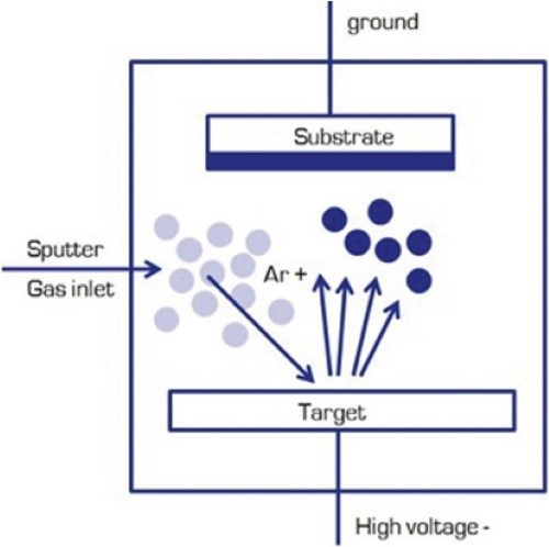 Figure 1. The Sputtering Process
This technique offers several advantages, including precise control over film thickness, high material purity, and the ability to deposit a wide range of materials. It is widely used in industries such as microelectronics, optics, and coating technology to create thin films with specific properties for various applications. Sputtering plays a crucial role in producing everything from semiconductor devices to optical coatings on lenses and mirrors. Its versatility and ability to deposit high-quality films make it a valuable tool in modern manufacturing and research.
How Sputtering Stacks Up: A Quick Comparison
| Feature | Sputtering | Evaporation | Electroplating |
|---|---|---|---|
| Film Quality | High density, excellent adhesion | Lower density, poorer adhesion | Varies, can be porous |
| Deposition Rate | 0.1-1 µm/min (varies by type) | 0.5-10 µm/min | Can be very high |
| Material Compatibility | Very wide (metals, ceramics, alloys) | Limited by evaporation temperature | Limited to conductive surfaces |
| Environmental Impact | Low (no hazardous chemical waste) | Low | High (toxic chemical waste) |
| Operational Cost | High (equipment, energy, targets) | Moderate | Low |
Advantages of Sputtering
Indeed, sputtering is a technique that brings a multitude of advantages to the realm of thin film deposition. Here are some notable examples.
- High Purity Deposition: It allows for the deposition of high-purity thin films since it does not involve chemical reactions. This makes it suitable for applications where material purity is critical, such as in microelectronics.
- Controlled Film Thickness: It provides precise control over the thickness of the deposited film, enabling the production of thin films with specific thickness requirements.
- Uniform Coating: Sputtering typically results in uniform film deposition across the entire substrate surface, ensuring consistency in film properties. This results in film thickness deviation typically less than ±5%, which is crucial for semiconductor manufacturing.
- Wide Material Compatibility: Sputtering can be used with a wide range of materials, including metals, semiconductors, ceramics, and even some polymers, making it versatile for various applications.
- Excellent Adhesion: Sputtered films often exhibit strong adhesion to the substrate, reducing the risk of delamination or peeling. This is because the sputtered atoms possess higher energy (around 10 eV) compared to evaporated atoms (around 0.1 eV), leading to better interfacial mixing.
- High-Density Films: The high packing densities of high-density films can lead to improved mechanical and electrical properties. Techniques like High-Power Impulse Magnetron Sputtering (HiPIMS) can produce exceptionally dense, pore-free coatings, which are critical for corrosion protection and advanced semiconductor barriers.
- Scalability and Flexibility: The technology is highly scalable, from research-scale samples to high-volume industrial production. It supports both batch processing and continuous roll-to-roll (R2R) production for flexible electronics, making it adaptable to various manufacturing needs
Disadvantages of Sputtering
However, sputtering is not without its challenges, and a comprehensive understanding of both its strengths and limitations is crucial for harnessing its full potential.
- Low Deposition Rate: Sputtering generally has a slower deposition rate compared to other techniques like chemical vapor deposition (CVD) or atomic layer deposition (ALD). This can be a limitation for high-volume production. However, it’s crucial to balance this with its unique strength: excellent composition control. Unlike some PVD methods (e.g., evaporation), sputtering reliably transfers the target’s stoichiometry to the film, making it indispensable for depositing multi-component alloys and compounds with precise chemical formulas, where accuracy is often more critical than speed.
- Target Erosion: During sputtering, the target material gradually erodes, reducing its lifespan and necessitating frequent target replacement. This is particularly pronounced in planar magnetron targets, which have a utilization rate of only ~30%. Rotary targets can improve this to ~80%, reducing waste and operational costs.
- Line of Sight Deposition: Sputtering is a line-of-sight process, which means that areas not directly exposed to the sputtered material may receive limited deposition. This can be a limitation for coating complex shapes. This remains a key challenge for coating intricate internal geometries, such as the deep pores of 3D foam structures used in next-generation catalysts or energy storage devices. While substrate rotation and fixture design can mitigate this, it adds complexity and cost.
- High Equipment Cost: Sputtering equipment can be expensive to purchase and maintain, which may be a barrier to entry for some facilities. This process typically requires the use of argon gas, which can add to operational costs. Costs are driven by the need for high-vacuum systems, powerful power supplies, and specialized targets.
- Heat Sensitivity: Some materials are sensitive to the heat generated during sputtering, which can limit their use with this technique. While traditional sputtering can heat substrates, modern magnetron sputtering techniques are designed to minimize this by confining electrons, thus reducing the thermal load on sensitive substrates .
Related reading: Advantages and Disadvantages of Ion Beam Sputtering
Conclusion
In summary, sputtering is a versatile and widely used thin film deposition technique with several advantages, including high purity, precise control, and uniformity. Yet, it also has limitations, such as slower deposition rates, high equipment costs, and heat sensitivity. The choice of deposition technique depends on the specific requirements of the application and the properties of the materials involved.
Sputtering remains a cornerstone technology in thin-film deposition. Its classic advantages—high purity, excellent adhesion, and material versatility—ensure its critical role in industries from microelectronics to advanced optics. While challenges like deposition rate and cost persist, ongoing advancements, such as HiPIMS and improved target designs, are actively expanding its capabilities. For applications demanding precise composition control, superior film quality, and environmental compliance, sputtering often presents an optimal solution, despite its higher initial investment.
Stanford Advanced Materials (SAM) is a leading supplier of a variety of sputtering targets and evaporation materials. Customization is also welcome. Send us an inquiry if you are interested.
Reference:
[1] Pujahari, R. (2021, June 8). Solar cell technology. ScienceDirect. Retrieved September 13, 2025, from https://www.sciencedirect.com/topics/chemical-engineering/sputter-deposition


