Key PVD Target Guide for 3nm/2nm Nodes: Selecting Cobalt & Ruthenium Barrier Layers
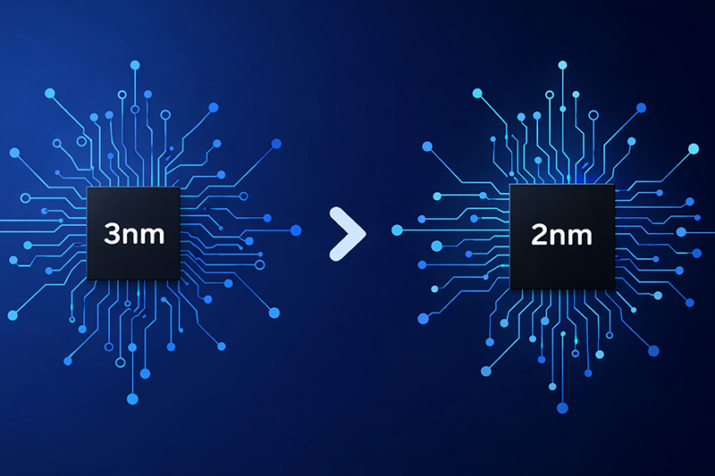
As the semiconductor industry advances beyond the 5nm node, conventional barrier/liner materials, such as Ta/TaN, are approaching their physical limits. This article provides a technical point of view of the two most promising successors: Cobalt (Co) and Ruthenium (Ru) PVD targets. We compare their material properties, process integration challenges, and selection criteria for advanced FinFET and GAA architectures, offering a clear roadmap for optimizing thin film performance at the atomic scale.
Introduction: The Material Revolution Beneath Moore’s Law
The relentless pursuit of Moore’s Law has shifted the bottleneck from lithography to interconnect and contact scaling. At the 3nm/2nm nodes, the increasing aspect ratio of features and the sheer density of interconnects expose the limitations of traditional Tantalum (Ta) / Tantalum Nitride (TaN) barrier layers. Their higher resistivity and less-than-ideal conformality in ultra-narrow vias and trenches result in increased RC delay, increased electromigration risks, and diminished device performance.
This has catalyzed a material revolution, moving the industry toward noble and near-noble metals. Cobalt (Co) and Ruthenium (Ru) have emerged as the frontrunners for next-generation barrier and liner applications. Selecting the optimal PVD target for these materials is no longer a mere procurement decision; it is a critical process integration choice that impacts yield, reliability, and performance.
Technical Comparison: Cobalt vs. Ruthenium
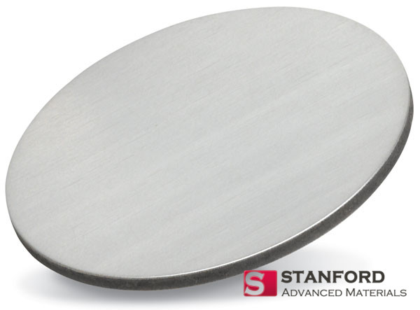
Cobalt Barrier Targets
Cobalt has seen rapid adoption in intermediate nodes for its superior properties:
- Lower Resistivity: ~6.24 μΩ·cm, significantly lower than Ta (~13.1 μΩ·cm) and TaN (~>200 μΩ·cm), reducing via resistance.
- Excellent Gap Fill Capability: Co demonstrates better reflow and bottom-up fill characteristics in high-aspect-ratio contacts compared to Ta, improving conformality.
- Enhanced Electromigration (EM) Resistance: It forms a robust interface with copper, effectively suppressing Cu diffusion and improving interconnect reliability.
However, Co presents distinct challenges:
- Oxidation Sensitivity: Cobalt is prone to forming native oxides, which can increase contact resistance if not carefully controlled via pre-clean and deposition environment.
- Adhesion to Dielectrics: Its adhesion to certain low-k dielectrics can be inferior to TaN, requiring interface engineering or adhesion layers.
- Target Purity & Microstructure: Impurities like oxygen or carbon in the Co target can lead to film defects and increased resistivity. A uniform, fine-grained target microstructure is essential for consistent, low-particle deposition.
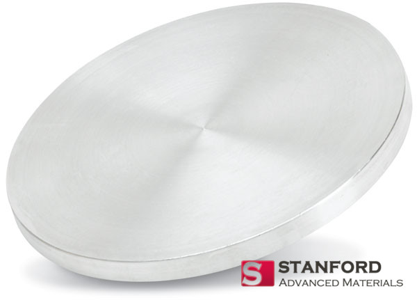
Ruthenium Liner PVD
Ruthenium is gaining attention for its revolutionary potential as a “linerless” liner or a direct plateable surface:
- The Ideal Liner for Direct Cu Plating: Ru‘s unique surface energy allows for direct, void-free electroplating of copper without a traditional PVD Cu seed layer, simplifying the process flow.
- Superior Diffusion Barrier Properties: Even in thin layers (<2nm), Ru provides an excellent barrier against Cu diffusion, a critical requirement for scaled interconnects.
- Thermal and Chemical Stability: Ru is highly resistant to oxidation and maintains stability at high temperatures, offering a robust interface.
The integration challenges for Ru include:
- Adhesion and Nucleation: Achieving uniform nucleation and strong adhesion on dielectrics can be difficult, often requiring optimized pre-treatment or very thin adhesion layers.
- Process Window Control: The deposition process for achieving a continuous, ultra-thin Ru film is narrow and requires precise control.
- Target Cost and Fabrication: High-purity Ruthenium targets are costly, and their fabrication (due to Ru‘s hardness and brittleness) demands specialized sputtering target manufacturing expertise.
Material Performance Comparison Table
| Property | Co (Cobalt) | Ru (Ruthenium) | Traditional Ta/TaN |
|---|---|---|---|
| Resistivity (μΩ·cm) | ~6.24 | ~7.1 | ~13.1 / >200 |
| Primary Function | Barrier/Liner | Liner/Direct Plate Barrier | Barrier |
| Key Advantage | Low Rc, Good Gap Fill | Enables Direct Cu Plating, Excellent Barrier | Proven Reliability, Good Adhesion |
| Integration Challenge | Oxidation, Dielectric Adhesion | Nucleation, Narrow Process Window | High Resistivity, Poor Conformality at Scale |
| Target Purity Requirement | ≥ 5N5 (99.9995%), Low O/C | ≥ 4N5 (99.995%), High Density | ≥ 4N (99.99%) |
If you require targets meeting these exacting specifications for your semiconductor project, contact us for a technical consultation.
Process Integration: Matching Target to Architecture
The choice between Co and Ru is also dictated by the specific transistor architecture and integration scheme.
- For FinFET and evolving GAA structures: The need for conformal coverage in tight, three-dimensional spaces is paramount. Co targets with optimized, highly uniform grain structure can provide the consistent step coverage required. The deposition process (power, pressure, substrate bias) must be tuned in tandem with the target‘s erosion profile to ensure uniformity.
- For advanced interconnects and buried power rails: The potential to eliminate the Cu seed layer with Ru liner PVD offers a significant simplification and scaling advantage. Here, the density and bonding integrity of the Ru target are critical to prevent arcing and achieve the low-defect, ultra-thin films needed.
The Supplier Selection Checklist: 5 Key Questions to Ask
Choosing the right partner for your advanced node sputtering target supply is as crucial as selecting the material itself. Beyond basic specifications, you must evaluate technical depth and manufacturing excellence.
- Purity & Microstructure Control: Can you demonstrate consistent target purity ≥5N5 for Co and ≥4N5 for Ru? How do you control grain size and orientation to ensure uniform erosion and film properties?
- Target Density & Bonding Integrity: What is your guaranteed target density (>99.5% for Ru)? What bonding technology (e.g., diffusion bonding, soldering) do you employ, and what is the typical thermal conductivity and bond strength to the backing plate? (At SAM, our proprietary HIP (Hot Isostatic Pressing) process guarantees >99.8% density, and our patented bonding technique ensures >95% bonding rate, maximizing thermal management and target life.)
- Process Support Data: Do you provide not just a target, but also baseline PVD process parameters and characterization data (film resistivity, step coverage, defect density) from partnered equipment OEMs or leading fabs?
- Customization & Co-Development Capability: Can you tailor target composition (e.g., Co alloying for specific properties), geometry, and bonding for our specific chamber and application?
- Quality & Traceability: Is your production line certified to relevant semiconductor standards (e.g., ISO, IATF)? Do you provide full material traceability from raw metals to finished target?
Conclusion
The transition to Co and Ru at the 3nm/2nm frontier is not merely a material swap. It is a holistic integration challenge where the quality of the PVD target is intrinsically linked to on-wafer performance. Success requires a supplier that is not just a manufacturer, but a materials science partner with deep expertise in high-purity metallurgy, advanced sputtering target manufacturing, and a proven track record in solving frontier problems.
At Stanford Advanced Materials (SAM), we combine decades of expertise in ultra-high purity materials with state-of-the-art fabrication and bonding technologies. Our targets are engineered not just to specification, but to enable your most demanding processes.
Ready to optimize your barrier and liner strategy for the next node?
Contact our technical sales team to discuss your specific requirements and receive a complimentary evaluation report on SAM‘s Cobalt and Ruthenium target solutions for your advanced node development.


