PVD Targets for DRAM & 3D NAND Manufacturing: From Capacitor Electrodes to Step Coverage
Abstract: The divergence in memory architecture between DRAM and 3D NAND Flash presents unique thin-film deposition challenges, directly impacting cost and performance. This article dissects the critical PVD target strategies for both technologies: the pursuit of seamless, high-aspect-ratio fill for DRAM capacitors, and the battle for conformal step coverage in 3D NAND’s towering staircases. We analyze material choices—from Al and TiN to advanced Ta-based barriers—and evaluate the economic imperative of maximizing target utilization as stack heights continue to climb.
Chiu, Yung-Yueh & Shirota, Riichiro. (2021). Technique for Profiling the Cycling-Induced Oxide Trapped Charge in NAND Flash Memories. Electronics. 10. 2492. 10.3390/electronics10202492.
Introduction
The relentless demand for higher density and lower cost-per-bit has driven memory manufacturing down two distinct but equally demanding paths. DRAM (Dynamic Random-Access Memory) scales laterally and vertically within a 2D plane, pushing capacitor deep trench (DT) and stack architectures to extreme aspect ratios. 3D NAND (Vertical NAND or V-NAND) escapes the planar limit by stacking memory cells vertically, creating vast “staircase” structures with re-entrant profiles. While the end goals differ, both rely on Physical Vapor Deposition (PVD) to deposit critical conductive and barrier layers. The choice of sputtering target material and its associated process window is a key lever for controlling device performance, yield, and ultimately, the cost structure of the memory chip.
DRAM Focus: Engineering the Capacitor Electrode
The heart of a DRAM cell is its capacitor, which must store enough charge in an ever-shrinking footprint. Modern high-aspect-ratio cylinder or trench capacitors demand flawless thin-film deposition.
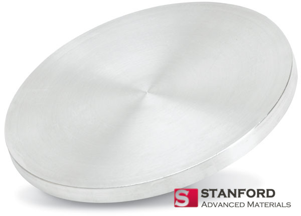
The Aluminum (Al) Target for Storage Node Electrodes:
- Role: Forms the primary conductive electrode. Its low resistivity and established etch chemistry are vital.
- Challenges: As aspect ratios exceed 50:1, achieving bottom-up, void-free fill becomes paramount. Traditional PVD struggles with overhang at the trench mouth, leading to pinch-off and voids.
- Target & Process Optimization: This requires a synergy between target and process. High-purity Al targets with fine, uniform grain structure ensure consistent flux. Processes like ionized PVD (I-PVD) are then employed, where argon ions bombard the target to create a high fraction of ionized Al atoms. These ions can be guided by an external field into the deep trench, improving sidewall coverage and bottom fill.
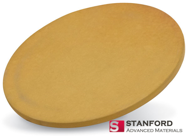
The Titanium Nitride (TiN) Target for Electrode & Barrier Layers:
- Role: Serves as a critical barrier layer (e.g., between the Al electrode and the dielectric) and as a electrode material itself in advanced structures.
- Challenges: Requires excellent conformality and low resistivity. Any discontinuity or high resistance in the TiN layer compromises capacitor performance.
- Target & Process Optimization: The stoichiometry and density of the TiN target are crucial. A dense, near-stoichiometric target yields a stable, low-resistivity film. Reactive sputtering from a pure Ti target in a N₂ atmosphere offers tunability, while sputtering from a pre-formed TiN compound target offers superior process stability and lower defect risk, especially for critical barrier applications.
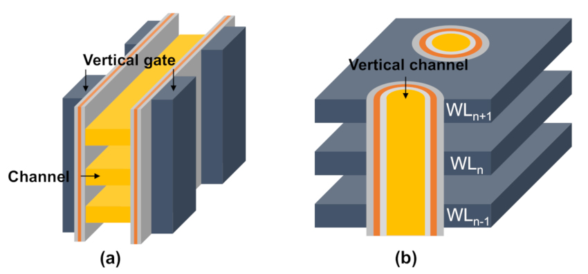
The 3D NAND Challenge: Conquering the Staircase
3D NAND fabrication involves etching and filling hundreds of layers of alternating materials, creating a structure akin to a skyscraper with deep, vertical channel holes and pronounced lateral staircases for word-line contacts.
The Step Coverage Imperative:
-
The staircase edge is where word-line metals must connect to the peripheral circuitry. Depositing a continuous, low-resistance barrier and metal liner over these extreme topography steps—with aspect ratios often >20:1—is the single greatest thin-film challenge in 3D NAND.
Tantalum (Ta) / Tantalum Nitride (TaN) Target Strategy:
- Role: The workhorse barrier/liner combination to prevent diffusion and provide adhesion for the subsequent tungsten (W) fill.
- Limitations of PVD: Conventional PVD suffers from “shadowing,” where the deposition flux cannot reach the bottom corners of high-aspect-ratio features, leading to poor step coverage and barrier failure.
- Advanced PVD Techniques: To overcome this, long-throw PVD and self-ionized plasma (SIP) PVD are employed. These techniques require targets with exceptional microstructure uniformity to maintain process stability at lower pressures and with specific plasma conditions. The erosion profile of the tantalum or tantalum nitride target must be tightly controlled to ensure consistent film properties over the target’s lifetime.
The ALD Alternative & Co-Existence:
Atomic Layer Deposition (ALD) offers near-perfect conformality and is increasingly used for the initial, ultra-thin barrier seed layer. However, ALD is slow and costly for thicker films. The prevailing strategy is a hybrid approach: an ultra-conformal ALD TaN base layer, followed by a thicker, more conductive PVD Ta layer to build up the liner. This makes the performance of the subsequent PVD Ta target—its purity and deposition rate—still critically important.
Cost Analysis
As 3D NAND layer counts soar past 200 and DRAM capacitors delve deeper, the economic model of sputtering targets shifts.
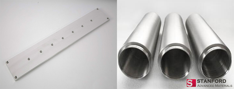
- The Utilization Factor: A planar target may only see 30-40% of its material consumed before erosion trenches necessitate replacement. For expensive metals like Ta, this is a significant cost contributor.
- Rotary Targets for Memory: Rotary cylindrical targets can increase utilization to 70-80% or higher by presenting a constantly rotating surface to the plasma. Their adoption in memory fabrication is a direct cost-saving measure.
- Lifecycle Cost Per Layer: The metric shifts from “cost per target” to “cost per deposited layer per wafer.” A target with higher utilization, longer life, and more stable deposition rates (enabled by superior bonding and uniform density) directly reduces the cost per layer stacked. This is non-trivial when multiplied by hundreds of layers across millions of wafers.
Further reading: Planar Targets VS. Rotatory Targets: Advantages and Disadvantages
Conclusion
The roadmap for DRAM and 3D NAND is a roadmap of increasing topological complexity. Success hinges on moving beyond simple material supply to a deep process-aware partnership. The optimal target strategy encompasses:
- Material Purity & Microstructure tailored for advanced PVD techniques (I-PVD, SIP-PVD).
- Advanced Target Design (like rotary targets) to maximize material utilization and lower cost-of-ownership.
- Hybrid Process Understanding to excel in the ALD/PVD integration schemes that define next-generation memory fabrication.
Facing specific deposition challenges in your memory production line?
Contact our technical team to discuss your DRAM capacitor or 3D NAND staircase requirements. We provide tailored target specifications and process integration support to optimize your film performance and total cost.


