Chemical Formula: BN
Catalog Number: ST0209
CAS Number: 10043-11-5
Purity: >99.5%
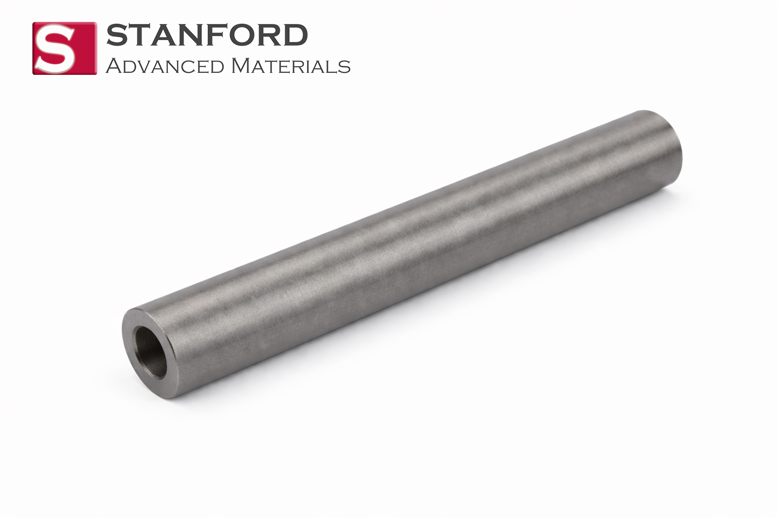
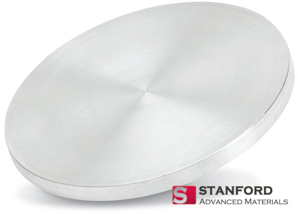
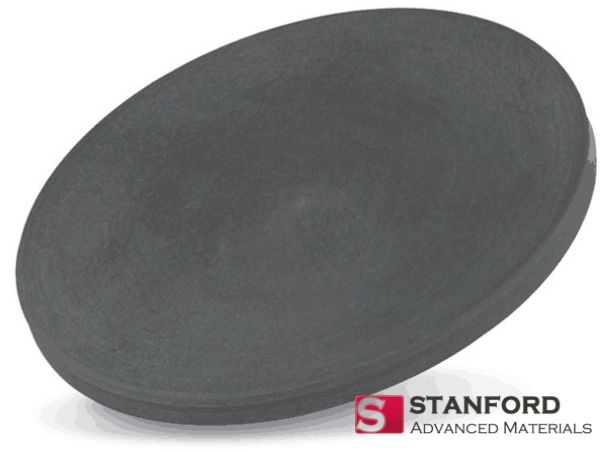
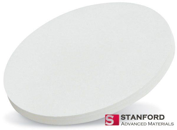
Shape: Discs, Plates, Column Targets, Step Targets, Custom-made
Boron nitride sputtering target is available in various forms, purities, sizes, and prices. Stanford Advanced Materials (SAM) is experienced in providing the highest quality BN target products.
 Boron Nitride Sputtering Target Safety Data Sheet
High Purity BN Ceramics for Thin-film Application
Stanford Advanced Materials (SAM) supplies high-purity boron nitride (BN) sputtering targets engineered for stable, high-efficiency thin film deposition. BN is a ceramic compound known for its exceptional thermal stability, electrical insulation, and non-stick properties, making it an ideal material for a wide range of advanced coating applications.
Our BN sputtering targets are offered in standard and customized dimensions, with optimized microstructure and density to ensure low particle generation and excellent film uniformity.
Related Product: Boron (B) Sputtering Target, Nitride Ceramic Target
| Property | Value |
|---|---|
| Material | Boron Nitride (BN) |
| Appearance | White, crystalline solid |
| Purity | 99.5%, 99.9% |
| Melting Point | ~3,000 °C |
| Theoretical Density | 2.25 g/cm³ |
| Sputtering Method | RF, RF-R |
| Bonding Options | Indium, Elastomer |
| Recommended Bonding | Elastomer (for thermal shock resistance) |
| Custom Sizes | Dia. 1″–6″, Thick. 0.125″–0.25″ |
Note: BN is a non-conductive ceramic and must be sputtered using RF power. It may decompose under aggressive conditions; use in reactive atmospheres is preferred.
Boron nitride sputtering targets are used in:
Semiconductor & Insulating Layers
Ideal for gate dielectrics, passivation layers, and insulating films in IC and MEMS fabrication.
Display & LED Devices
Optical and thermal barrier coatings in OLED, LCD, and laser diode manufacturing.
Photovoltaics & Transparent Electronics
UV-resistant, thermally stable dielectric barriers.
High-Temperature Coatings
Protective layers for crucibles, tools, and components operating above 1,500 °C.
Nanotechnology
BN nanotubes and 2D h-BN layers offer high mechanical strength and thermal conductivity for next-gen devices.
BN targets are typically bonded before installation to prevent cracking during sputtering. We offer:
Elastomer Bonding – Recommended for BN due to its brittleness and low thermal conductivity.
Indium Bonding – Optional, but use caution with high-temperature cycling.
Custom Backing Plates – Available in copper, molybdenum, stainless steel, and more.
Learn More About Bonding Services →
Each boron nitride target is vacuum-sealed and securely packaged with foam inserts in a clean environment to prevent contamination and mechanical damage. All shipments include full labeling and traceability.
SAM’s high quality BN sputtering target is available in various forms, purities, sizes, and prices. We specialize in producing high purity thin film coating materials with the highest possible density and smallest possible average grain sizes for use in semiconductor, chemical vapor deposition (CVD) and physical vapor deposition (PVD) display and optical applications. Please send us an inquiry for current pricing on sputtering targets and other deposition materials not listed.
Submit your review | |
We’ve used SAM’s BN targets in multiple PVD tools for high-temp barrier coatings, and the performance has been exceptional. No cracking, stable power handling, and very clean films. Highly recommend elastomer bonding for longer service life.
The dimensions were exactly as ordered, and the packing was well above standard. Zero chipping or contamination. SAM’s BN targets are now our go-to for insulating oxide layers.
Great stuff wish I found out about this stuff years ago.