(949) 407-8904 Mon - Fri 08:00 - 17:00 1940 East Deere Avenue, Suite 100, Santa Ana, CA 92705, USA

Cornerstone Articles

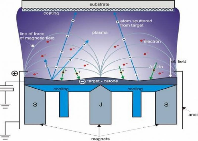
Stanford Advanced Materials (SAM) Corporation is a global supplier of various sputtering targets such as metals, alloys, oxides, ceramic materials. We update every week about news and knowledge of sputtering targets and evaporation materials. Here are the cornerstone articles we published previously, if you want to see all the news, please click here.

15
Jan

An Overview of Magnetron Sputtering

An Overview of Magnetron Sputtering Magnetron sputtering, a physical vapor deposition (PVD) process, is a main thin film deposition method for manufacturing semiconductors, disk drives, CDs, and optical devices. Magnetron sputtering has the advantages of high speed, low temperature, and low damage. In this article, let’s take a look at the definition, working principle, and...
Continue Reading
Metal Encyclopedia Seventeen Rare Earth Elements Introduction
30
Oct

Metal Encyclopedia: Seventeen Rare Earth Elements Introduction

Rare-earth element is a general term for 17 elements of lanthanides as well as scandium and yttrium in the chemical periodic table. Scandium and yttrium are included in rare earth element because they are often symbiotic with lanthanide elements in mineral deposits, and thus have similar chemical properties. Rare earth materials are important for many...
Continue Reading
10
Sep

Everything You Need to Know About Sputtering Targets

1. Introduction to Sputtering Targets Sputtering targets are significant commodities for thin-film industries like electronics, optics, and energy sectors. Simply put, a “sputtering target” is the target material utilized for sputtering, a form of physical vapor deposition (PVD). During the PVD process, atoms from a solid target are removed and ejected upon impact by high-energy...
Continue Reading
What is Physical Vapor Deposition
07
Jul

What is Physical Vapor Deposition (PVD)?

What is PVD Coating Technology? Physical Vapor Deposition (PVD) is a thin film preparation technique that physically vaporizes the surface of a material source (solid or liquid) into gaseous atoms, molecules, or partially ionized into ions under vacuum conditions. Then, a film having a specific function is deposited on the surface of the substrate by...
Continue Reading
17
Jan

Detailed Introduction to Three Generations of Semiconductor Materials

What are the Three Generations of Semiconductor Materials? The first generation of semiconductor material The first generation of semiconductor materials mainly refers to silicon (Si) and germanium (Ge) materials. In the 1950s, Ge dominated the semiconductor market and was mainly used in low-voltage, low-frequency, medium-power transistors and photodetectors. However, Ge semiconductor devices were inferior in...
Continue Reading
25
Sep

Top 10 Sputtering Target Materials that Can Withstand High Temperatures

Sputtering is a widely used process in various industries, from electronics to optics. High-temperature sputtering targets are essential for applications that require materials to perform under extreme conditions. Here are the top ten sputtering target materials known for their ability to withstand high temperatures, listed from highest to lowest melting point. 1. Tungsten Sputtering Target...
Continue Reading
cobalt-sputter-target-a-comprehensive-guide
17
Jan

Cobalt Sputter Target: A Comprehensive Guide

Introduction In the realm of advanced materials and cutting-edge technologies, cobalt sputter targets have emerged as key players, revolutionizing various industries. This article aims to delve into the intricacies of cobalt sputtering targets, exploring their applications, manufacturing process, and significance in the world of thin-film deposition. Understanding Cobalt Sputter Targets Cobalt sputter targets are vital...
Continue Reading
03
Jul

Planar Targets VS. Rotatory Targets: Advantages and Disadvantages

The sputtering target materials commonly found on the market can be divided into planar targets and rotatory targets according to their shapes. Want to know what are their advantages and disadvantages? Keep on reading this post. Planar Sputtering Target Although rotary targets have developed in recent years, the mainstream shape of the sputtering target is still the planar type. Advantages...
Continue Reading
Major Problems and Answers in Coating Technology
19
Nov

Major Problems and Answers in Coating Technology

1. What types of coating technology can be divided into? (1) Vacuum coating (2) Electroplating (3) Chemical reaction (4) Heat treatment (5) Physical or mechanical treatment 2. What are the applications of plasma technology in surface technology? Sputter deposition: Sputtering is the use of high-speed ions to strike a solid sputter target, causing surface molecules...
Continue Reading
electron beam evaporation
01
Nov

An Overview of Electron Beam Evaporation

Electron Beam Evaporation – Definition Electron beam evaporation, or E-beam evaporation, is a type of physical vapor deposition (PVD) technique, which directly heats the evaporation material (usually pellets) by using an electron beam under vacuum, and transports the vaporized material to the substrate to form a film. Electron Beam Evaporation – Working Processes Electron beam evaporation...
Continue Reading
1 2 3