Fabrication of Niobium Nitride Thin Films: A Critical Analysis of Deposition Methodologies
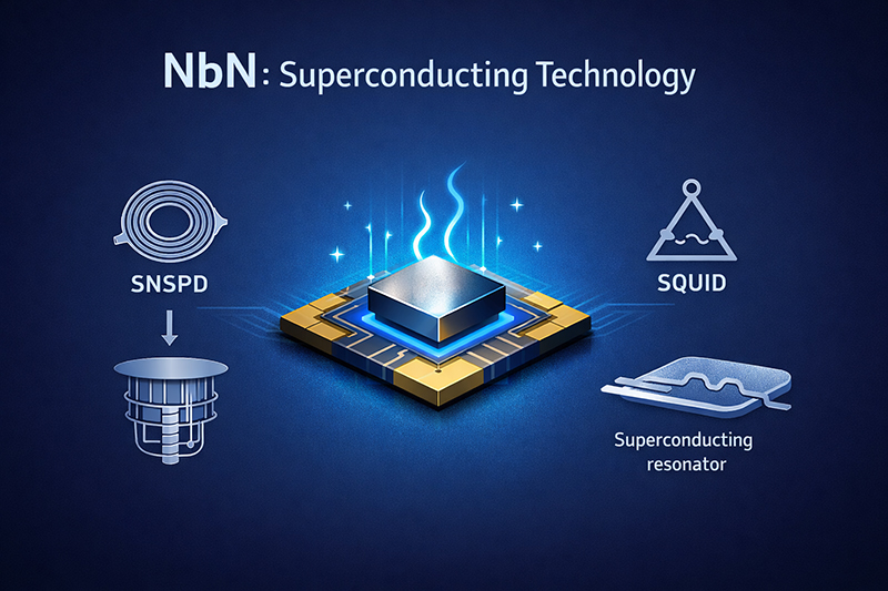
Niobium nitride (NbN) is widely used in superconducting devices, and its performance depends largely on how its thin film is formed. In this article, we look at four main methods: reactive magnetron sputtering, atomic layer deposition (ALD), pulsed laser deposition (PLD), and chemical vapor deposition (CVD). We explain how process details like gas mix, temperature, and power influence the film quality. We also offer a straightforward guide to the trade-offs each method brings, with practical numbers and simple examples to help you decide which technique fits your needs best.
Reactive Magnetron Sputtering
Reactive magnetron sputtering is a long-used and trusted method to make NbN films. In this method, a niobium metal target is bombarded by plasma in a mix of argon and nitrogen. The sputtered atoms then settle on a substrate to form the film.
A common challenge here is managing the reactive process. If you use too little nitrogen, the film may be deposited quickly but will not be fully stoichiometric. This means the resistivity can be higher and the film may not become superconducting at the best temperature. Increasing the nitrogen flow helps the film form the desired phase, but it also reduces the rate by around 40-60% because the target begins to form a nitride layer—a problem sometimes called target poisoning. Experienced technicians typically adjust the nitrogen flow to be about 5-10% lower than the level that causes rapid rate decline.
Temperature is also key. For a film with good crystal alignment, substrates like magnesium oxide (MgO) or aluminum oxide (Al₂O₃) are heated to 300–450°C. When working with silicon circuits, lower temperatures (less than 200°C) are used. In these cases, a moderate radio frequency bias (around –20 to –60 volts) is applied to help create a dense film. However, using a bias can introduce stress into the film, which must be balanced to avoid cracking or poor adhesion.
Atomic Layer Deposition
Atomic Layer Deposition, or ALD, offers very accurate control over film thickness. This is important when you need films only a few nanometers thick, such as in superconducting nanowire single-photon detectors. ALD works by exposing the substrate to alternate chemical vapors, which react on the surface one layer at a time.
When using ALD, the choice of chemicals matters. For instance, processes using niobium pentachloride with ammonia need higher temperatures (above 350°C) and may produce corrosive byproducts. On the other hand, using metalorganic compounds with plasma-activated nitrogen can allow growth at a lower temperature (about 250–300°C). In ALD, the film typically grows about 0.08–0.1 nm per cycle. In practice, a small change of one nanometer may be enough to change a device’s switching current by over 20%.
One drawback of ALD is its slow speed—usually below 3 nm per minute. There is also a risk of impurities such as carbon or oxygen getting into the film if the purge steps are not done carefully. This method is best used for projects where every nanometer counts rather than for fast, mass production.
Pulsed Laser Deposition
Pulsed Laser Deposition uses high-powered laser pulses to vaporize material from a target, which then winds up as a film on the substrate. This method is great for keeping the film’s composition exactly the same as the target. A burst of high-energy particles, typically in the range of 1–100 electron volts, hits the substrate and encourages a dense, well-adhered film.
For instance, when depositing NbN, the substrate is usually kept at a moderate temperature between 500 and 700°C. This helps in forming films that are well-aligned with the underlying material, especially on complex substrates. However, one must be cautious. The laser can create little droplets or particulates from the target. These tiny particles can lead to surface defects, which are problematic for devices that require a very smooth surface.
To reduce these issues, many labs use off-axis deposition settings or filters. Yet, the deposition area remains small due to the focused nature of the plume. This method is most suitable for small-scale research or prototyping where precise stoichiometry is more important than covering large areas.
Chemical Vapor Deposition
Chemical Vapor Deposition, or CVD, comes in a few flavors. The traditional thermal CVD uses high temperatures—often above 900°C—to trigger chemical reactions on the substrate surface. Such high temperatures are usually not acceptable for superconducting work.
Modern techniques include Plasma-Enhanced CVD and Metalorganic CVD. Plasma-Enhanced CVD can deposit films at lower temperatures around 400–600°C using gases such as niobium fluoride or niobium chloride. But the use of halogens makes post-treatment necessary to remove unwanted elements. Metalorganic CVD uses different precursors and works below 500°C. This method provides excellent step coverage, which is useful for coating surfaces with complex shapes. One must be aware, though, that incomplete breakdown of the organic parts can leave behind carbon that lowers the superconducting performance.
Each of these CVD variants has its own niche based on the geometry of the substrate and the required purity of the film.
Comparative Summary and Decision Framework
Choosing the right deposition method is all about balancing trade-offs. Here are some simple points to consider:
• In reactive magnetron sputtering, keeping a tight grip on the nitrogen levels and substrate temperature is important. This is a reliable method for applications such as microwave circuits or large-area sensors.
• Atomic layer deposition offers precise control when you need films only a few nanometers thick, as in superconducting nanowires. Its slow rate is its main drawback.
• Pulsed laser deposition is useful when maintaining the exact chemical makeup is key. However, a small area and the risk of particulates make it more suited for lab-scale experiments.
• Modern chemical vapor deposition techniques are chosen when one must cover complex surfaces. The controlled temperature and step coverage are big pluses, even though impurity control is crucial.
It is best to look at the specific requirements of your device—like the desired temperature range, film thickness, and surface geometry—to choose the right method. Many research groups even mix techniques to get a more balanced result.
| Method | When to Choose It | Practical Considerations |
|---|---|---|
| Magnetron Sputtering | For most device applications requiring consistent, high-quality films on flat substrates. | Equipment availability is excellent. Process development is straightforward. Scalable to production. |
| ALD | When thickness must be controlled at the atomic level or when coating 3D nanostructures. | Slow deposition rate (100-300 nm/hour). Requires specialized precursors and equipment. |
| PLD | For fundamental materials research or when growing epitaxial films with perfect stoichiometry. | Small-area deposition. Requires single-crystal targets. Throughput is low. |
| CVD | For coating non-planar geometries or when integrating with existing CVD-based processes. | Precursor handling can be challenging. May require high temperatures unless using plasma enhancement. |
Conclusion
Niobium nitride thin films remain a cornerstone in the realm of superconducting devices. Each deposition method comes with its own set of advantages and shortcomings. In simple terms, reactive magnetron sputtering offers steady production while atomic layer deposition gives you the precision needed for nanoscale work. Pulsed laser deposition remains a favorite for keeping the film composition true to form, and the modern variants of chemical vapor deposition ensure even tricky surfaces are well coated.
In our long experience working with these processes, we have seen that no single method fits all needs. Sometimes, combining ideas from different processes, such as seeding a sputter growth with an ALD layer, can yield the best film quality. For anyone working on next-generation superconducting electronics, a careful look at the numbers and trade-offs can save both time and materials.
For trusted and high-quality niobium nitride materials, please refer to Stanford Advanced Materials (SAM).


