Typical Materials of the Third Generation Semiconductors
The third generation of semiconductor materials are those materials with a wide bandgap (Eg≥2.3eV). They usually have high breakdown electric field, high thermal conductivity, high electron saturation rate and higher radiation resistance. That is why they are used for making high temperature, high frequency, radiation-resistant and high power devices. Typical materials are silicon carbide (SiC), gallium nitride (GaN), aluminum nitride (AlN), and zinc oxide (ZnO).
Silicon Carbide Single Crystal Semiconductor
The technological maturity of silicon carbide is the highest in the field of wide bandgap semiconductor materials and is the core of wide bandgap semiconductors. Silicon carbide is a semiconductor compound with a wide bandgap (Eg: 3.2 eV), a high breakdown electric field (4 x 10⁶ V/cm), and a high thermal conductivity (4.9 W/cm.k).
Further Reading: An Overview of Silicon Carbide Ceramic Materials
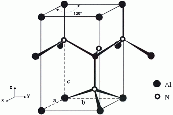
Gallium Nitride Semiconductor
The GaN material is an III-V compound semiconductor material synthesized by Johason et al. in 1928. GaN materials have good electrical properties, wide bandgap (3.39eV), high breakdown voltage (3×10⁶V/cm), high electron mobility (room temperature 1000cm2/V·s), high heterojunction charge density (1× 1013cm-2), etc. Therefore, it is considered to be the most preferred material for studying short-wavelength optoelectronic devices and high-temperature high-frequency high-power devices.
GaN devices can operate at higher frequencies, higher power, and higher temperatures than silicon, gallium arsenide, germanium, and even silicon carbide devices. In addition, GaN devices can be used in the high-frequency range from 1 to 110 GHz, covering mobile communications, wireless networks, point-to-point and point-to-multipoint microwave communications, and radar applications.
In recent years, Group III nitrides represented by GaN have received extensive attention due to their application prospects in the field of optoelectronics and microwave devices. As a semiconductor material with unique optoelectronic properties, GaN applications can be divided into two parts: GaN semiconductor materials can replace some silicon and other compound semiconductor materials with excellent performance under high temperature and high frequency, high power operating conditions; develop new optoelectronic applications with the unique properties of GaN semiconductor materials with wide band gaps and blue light excitation.
Aluminum Nitride Semiconductor
Aluminum nitride is a Group III nitride with a direct band gap of 0.7 to 3.4 eV and can be widely used in the field of optoelectronics. Compared with materials such as gallium arsenide, it covers a larger spectral bandwidth, so it is especially suitable for applications from deep ultraviolet to blue light. What’s more, Group III nitrides have good chemical stability, excellent thermal conductivity, high breakdown voltage, and low electrical constants, making it possible to operate at higher frequencies, higher power, higher temperatures and harsh environments. Therefore, aluminum nitride is a promising semiconductor material.
Further Reading: Introduction to Aluminum Nitride Semiconductor
Zinc Oxide Semiconductor
Zinc Oxide is both a wide bandgap semiconductor and a multifunctional crystal with excellent photoelectric and piezoelectric properties. It is suitable for the fabrication of high-efficiency optoelectronic devices such as blue, ultraviolet light and detectors. It can also be used in the manufacture of gas sensing devices, surface acoustic wave devices, transparent high-power electronic devices, window materials for luminescent displays and solar cells, and varistor and piezoelectric conversion.
Conclusion
Thank you for reading our article and we hope that it can help you better understand the third generation of semiconductor materials. If you want to know more about semiconductors, we would like to advise you to visit Stanford Advanced Materials (SAM) for more information.
Further Reading: Detailed Introduction to Three Generations of Semiconductor Materials


