P-type & N-type Silicon Semiconductors
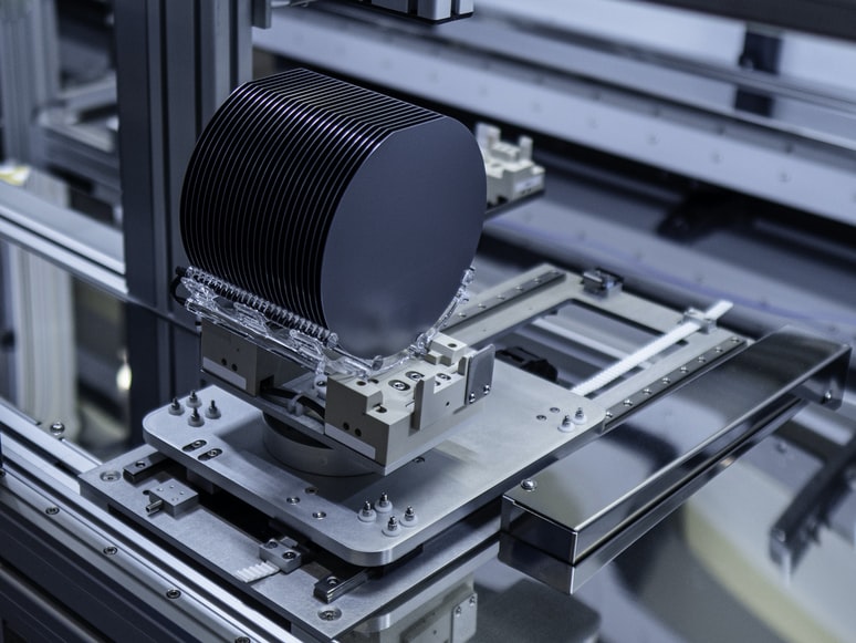
Semiconductors form the foundational backbone of modern electronics. Their most critical applications are in computers, smartphones, and virtually all digital circuits. Silicon, the predominant semiconductor material, is favored not only for its abundance in nature (primarily found in sand and quartz) but also for its unique and adaptable electronic structure.
Another very important thing to note about silicon is the impact of doping, a process in which impurities are introduced to enhance the value of an intrinsic semiconductor. Read on to learn more details about doping in silicon semiconductors.
Structure of Silicon
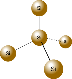
Similar to carbon, a silicon atom has four valence electrons, enabling it to form a stable crystalline lattice with a diamond structure. High-purity silicon has a shiny, metallic luster but is not a metal. In its pure form (known as intrinsic silicon), it has very few mobile charge carriers at room temperature. Consequently, its electrical conductivity is substantially lower than that of metals but higher than that of insulators, defining it as a semiconductor.
Types of Semiconductors
As previously mentioned, semiconductors are defined by their electrical conductivity, which is intermediate between conductors and insulators. This property is not fixed but can be precisely tuned through doping, leading to the two main categories discussed below.
Intrinsic Semiconductors
An intrinsic semiconductor is a high-purity material, such as silicon or germanium, whose semiconducting properties arise solely from the material itself without any impurity addition. Another name for this type of semiconductor is undoped semiconductors or i-type semiconductors. These are chemically pure semiconductors. In these semiconductors, electrons have energies in only certain bands. The energy bands correspond to a large number of discrete quantum states of electrons. Also, note that the distribution and population of bands in semiconductors is another factor that distinguishes them from metals.
For clarity, the valence band of electrons in metals is typically almost filled under normal conditions, but in semiconductors, only a few electrons exist in the conduction band, just above the valence band. Insulators, on the other hand, have nearly no free electrons, which is why they can’t conduct electricity. Also, in intrinsic semiconductors, the number of holes is equal to the number of excited electrons.
Extrinsic Semiconductors
Extrinsic semiconductors are created by deliberately introducing specific impurity atoms (dopants) into the crystal lattice of an intrinsic semiconductor. This process, called doping, fundamentally alters its electrical properties by increasing the number of free charge carriers.
Based on the type of dopant used, extrinsic semiconductors are categorized into two distinct types: N-type and P-type, which serve as the fundamental building blocks of modern electronic devices.
Doping in Semiconductor Production
Having defined intrinsic semiconductors, we now turn to the process that makes them technologically useful: doping. Doping is commonly used in semiconductor production to introduce impurities into an intrinsic semiconductor so as to modulate its electrical, optical, and structural properties. As explained above, doping silicon semiconductors produces the P-type and N-type silicon semiconductors.
The primary effect of doping is a dramatic increase in electrical conductivity by significantly raising the number of majority charge carriers (electrons in N-type, holes in P-type). In standard extrinsic semiconductors, conductivity is orders of magnitude higher than in intrinsic silicon. (The term “degenerate” refers to a specific, extreme case of doping where the semiconductor behaves like a metal, and mentioning it in an introductory text may be an unnecessary complication.)
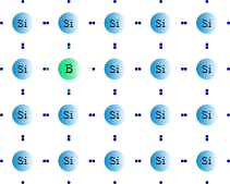
P-Type Semiconductor
With the concept of doping established, we can explore the two distinct types of extrinsic semiconductors. The first is P-type. P-type semiconductors are created by doping silicon with atoms from Group III (e.g., boron or gallium), which have one fewer valence electron than silicon. When a boron atom replaces a silicon atom in the lattice, it cannot form four complete covalent bonds, creating a hole—a localized deficiency of an electron. This hole can readily accept an electron from a neighboring silicon atom. The movement of electrons from neighboring atoms to fill this hole is equivalent to the hole itself moving in the opposite direction. This mobile hole acts as a positive charge carrier. It is critical to note that the crystal remains electrically neutral overall; “P-type” denotes that the majority carriers are positive holes, not that the material has a net positive charge.
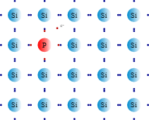
N-Type Semiconductors
N-type semiconductors are produced by doping silicon with atoms from Group V (e.g., phosphorus or arsenic). These dopant atoms have one more valence electron than silicon. Upon integration into the silicon lattice, the extra phosphorus electron is only weakly bound and can easily be excited into the conduction band, becoming a mobile negative charge carrier. In N-type semiconductors, electrons are the majority carriers. As with P-type, the material itself is electrically neutral.
Conclusion
The two types of silicon semiconductors are P-type and N-type semiconductors. These extrinsic semiconductors possess enhanced properties, which make them very useful in the electronic manufacturing industry.
Thank you for reading our article and we hope that it can help you better understand silicon semiconductors. If you want to know more about semiconductor materials, we would like to advise you to visit Stanford Advanced Materials (SAM) for more information.


