3 Factors Affecting the Deposition Rate in Magnetron Sputtering
Magnetron sputtering is a physical vapor deposition method that allows the deposition of various materials, including metals, oxides, ceramics and etc., by using a specially formed magnetic field applied to a diode sputtering target. The deposition rate, or the film formation rate, is an important parameter that measures the effectiveness of the magnetron sputtering machine.
In modern applications, from semiconductor fabrication to cutting-edge fusion reactor materials, achieving and controlling a precise deposition rate is not just about efficiency—it’s about reproducibility, film quality, and cost-effectiveness.
There are several influencing factors of the deposition rate, including the type of the ambient air, the working pressure, the temperature of the sputtering target, the strength of the magnetic field, and so on. But today, we’re going to talk about the 3 important factors affecting the deposition rate in magnetron sputtering: the sputtering voltage, current, and power.
The Interplay of Voltage, Current, and Power: A Quick Overview
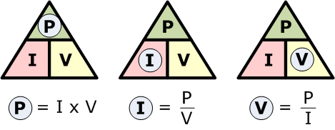
Before diving in, it’s crucial to understand that voltage (V), current (I), and power (P) are not independent variables. They are intrinsically linked by the relationship P ≈ V × I. Adjusting one invariably affects the others, making the control of magnetron sputtering a balancing act to achieve the desired plasma characteristics and deposition outcome.
1. Sputtering Voltage (V)
Experiment results have shown that the effect of sputtering voltage on film formation rate has such a rule: The higher the voltage, the faster the sputtering rate, and the effect is tempered and gradual over the range of energies required for sputter deposition. Among the factors affecting the sputtering coefficient, after the sputtering target material and the sputtering gas, the discharge voltage really matters. Generally, in the normal process of magnetron sputtering, the higher discharge voltage has a larger sputtering coefficient, which means the incident ions have higher energy. Therefore, the atoms of the solid target are easier to be sputtered out and deposited on the substrate to form a film.
The voltage’s primary role is to accelerate ions from the plasma toward the target, imparting kinetic energy. This energy must exceed the target material’s specific “sputtering threshold” (typically 10-30 eV) to eject atoms. Once above this threshold, the yield (atoms ejected per ion) increases with voltage . However, this is not a linear relationship indefinitely. Excessively high voltages can lead to problems like gas incorporation in the film and increased secondary electron emission, which can steal energy from the sputtering process and reduce its efficiency.
Beyond just DC voltage magnitude, modern pulsed techniques like High-Power Impulse Magnetron Sputtering (HiPIMS) exploit ultra-high voltage pulses (hundreds to thousands of volts) to create extremely dense plasmas . Recent research on “dual-pulse HiPIMS” shows that using a short, high-voltage “ignition pulse” followed by a lower-voltage “working pulse” can optimize the discharge, leading to higher ionization without necessarily increasing the average voltage, thereby offering a more nuanced control over the process .
2. Sputtering Current (I)
The sputtering current of the magnetron target is in direct proportion to the ion current of the surface of the sputtering target, so it is also an important factor that affects the sputtering rate. There is a common law of magnetron sputtering that the deposition rate is fastest under the optimum gas pressure (according to different sputtering targets and different sputtering projects). Therefore, on the premise that the film quality won’t be affected and the customer’s requirements can be satisfied, it is appropriate to consider the optimum value of the gas pressure from the sputtering yield. There are two ways to change the sputtering current: change the working voltage or change the working gas pressure.
While voltage determines if and how efficiently atoms are ejected, the sputtering current directly determines the number of ions bombarding the target per unit time. A higher ion current density leads to more sputtering events, thus directly increasing the deposition rate. This is why the deposition rate is often roughly proportional to the target current.
In high-current scenarios like HiPIMS, a phenomenon known as “self-sputtering” can occur. Here, the ionization of the sputtered target material itself becomes so high that ionized metal atoms are attracted back to the target. This “back-attraction” is a primary reason why HiPIMS, despite its superior plasma density and film quality, often has a lower deposition rate compared to DC magnetron sputtering (DCMS). Innovations like dual-pulse HiPIMS aim to mitigate this by using a high current to ignite the plasma but then lowering the voltage to reduce back-attraction, successfully demonstrating a 3-fold increase in the deposition rate of CrN films compared to traditional HiPIMS.
Sputtering Power (P)
The effect of the sputtering power on the deposition rate is similar to the sputtering voltage. In general, increasing the sputtering power of the magnetron target can increase the film formation rate. This is, though, not a universal rule. In the case that the sputtering voltage of the magnetron target is low (for instance, around 200 volts) and the sputtering current is high, although the average sputtering power is not low, the ions cannot be sputtered and cannot be deposited. The prerequisite is that the sputtering voltage applied to the magnetron target is require to be sufficiently high so that the energy of the working gas ions in the electric field between the cathode and the anode is sufficiently greater than the “sputtering energy threshold” of the target.
Power is the product of voltage and current, making it a comprehensive parameter that reflects the total energy input into the plasma. In many industrial processes, especially with DCMS, power is the primary control knob. Increasing power typically increases both the ionization degree and the flux of ions to the target, leading to a higher deposition rate. The key caveat, as your original text noted, is that power must be delivered above the sputtering threshold voltage to be effective. Furthermore, the efficiency of converting power into deposited material varies greatly with the discharge mode.
- – DCMS: Offers high deposition rates but lower ionization.
- – HiPIMS: Provides high ionization (often >50%) for denser films, but at the cost of rate due to back-attraction
- – Emerging Techniques (like Dual-Pulse HiPIMS): Aim to achieve a “sweet spot” with better ionization than DCMS and better rates than traditional HiPIMS, optimizing power utilization for specific outcomes.
Conclusion
From the above discussion, you can see that voltage, current and power actually interact with each other. The deposition rate in magnetron sputtering is never affected by one of them but all of them.
Optimizing the deposition rate is a complex interplay of fundamental parameters and advanced techniques. It involves balancing the direct relationship of current and power with rate against the voltage-dependent efficiency and ionization degree. The choice of technique (DCMS, HiPIMS, or its advanced variants) inherently sets a baseline for this trade-off between rate and film quality. Furthermore, external factors like magnetic field configuration and process gas (e.g., using Helium for porous films or Ar-Ne mixtures for specific properties ) are critical co-factors. Ultimately, the “best” parameters are dictated by the specific application—whether the priority is maximum throughput, ultimate film density, or conformal coverage of complex structures.
Want to know the best parameters of these three factors for your project? Please send us an inquiry. The experienced team from Stanford Advanced Materials will give you a satisfactory solution for your project.
Stanford Advanced Materials has been a global sputter coating manufacturer since 1994. Please visit https://www.sputtertargets.net/ for more information.


