Home
Product
Sputtering Target
By Chemical Elements
Evaporation Materials
By Evaporation Materials
By Chemical Elements
Bonding Service
Indium Target Bonding Service
OFHC Copper Backing Plates
Elastomeric Target Bonding Service
Planar Targets
Evaporation Sources
Thermal sources
E-Beam Source Used Crucibles
3D Printing Powder
Crystal Substrates
Thermal Spraying Coating
Application
Architectural, Automotive Glass & WEB Coating
Semiconductor Materials
Hardware & Decorative Coatings
Optics Coatings
Solar
Electronics
FAQ
About Us
NEWS
Blogs
Industry News
Most Popular
Contact Us
(949) 407-8904
Mon - Fri 08:00 - 17:00
1940 East Deere Avenue, Suite 100, Santa Ana, CA 92705, USA
Get A Quote
Home
Products
Sputtering Targets
By Material Types
By Chemical Elements
Evaporation Materials
By Material Types
By Chemical Elements
Precious Metals
Gold Sputtering Target
Silver Sputtering Target
Platinum Sputtering Target
Gold Evaporation Materials
Evaporation Source
Thermal Sources
Alumina Boat
E-Beam Source Used Crucibles
Graphite Crucible
Tungsten Crucible
Boron Nitride Crucible
Zirconia Crucible
Crystal Substrates
Calcium Carbonate Crystal
Barium Titanate Crystal
Rutile Titanium Dioxide Crystal
3D Printing Powders
Thermal Spraying Coating
Targets
By Target Shapes
Planar Sputtering Target
Rotary Sputter Target
Rare Earth Targets
Erbium Sputtering Target
Praseodymium Sputtering Target
Pure Metal Targets
Gold Sputtering Target
Iridium Sputtering Target
Aluminum Target
Alloy Targets
Ti/W Sputtering Target
Mo/Nb Alloy Rotary Target
Nb/Ti Sputtering Target
Oxide Targets
SiO2 Sputtering Target
Magnesium Oxide Target
Aluminum Oxide Sputtering Target
Nitride Targets
TiN Sputtering Target
AlN Sputtering Target
Boron Nitride Sputtering Target
Fluoride Targets
MgF2 Sputtering Target
LiF Sputtering Target
Carbide Targets
Silicon Carbide Sputtering Target
Fe3C Sputtering Target
Pellets
Pure Metal Pellets
Gold Evaporation Materials
Alloy Pellets
Oxide Pellets
Nitride Pellets
Niobium Nitride Evaporation Materials
Fluoride Pellets
Magnesium Fluoride Evaporation Materials
Carbide Pellets
Iron Carbide Evaporation Materials
Silicide Pellets
Sulfide Pellets
Boride Pellets
Selenide Pellets
Services
Target Bonding
Indium Bonding
Copper Backing Plates
Elastomeric Bonding Service
Target Recycling
Applications
Solar
CIGS Sputtering Target
Semiconductors
Electronics
Lithium Niobate Sputtering Target
Optics Coatings
Hardware & Decorative Coatings
Automotive Glass & WEB Coating
About
Blogs
Cornerstone Articles
What is Physical Vapor Deposition (PVD)?
What is Chemical Vapor Deposition (CVD)? The Ultimate Guide
Glossary
Terms & Conditions
MSDS Listings
Privacy Policy
Friend Links
FAQ
Inquiry
Category
Industrial News
January 27, 2026
Julissa Green
Blog
,
Comparison
,
Industrial News
The Clock is Ticking on ITO. Is AZO Finally the Answer?
Here’s a fact that keeps display execs up at night: Your entire transparent electrode supply chain...
January 9, 2026
Julissa Green
Blog
,
Guides & How-to
,
Industrial News
Semiconductor Target TCO Analysis: Boosting Utilization by 30% via Design & Bonding
Abstract: In semiconductor manufacturing, the cost of a PVD sputtering target extends far beyond its purchase...
December 30, 2025
Julissa Green
Applications
,
Blog
,
Industrial News
,
Specific Materials
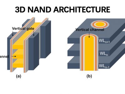
PVD Targets for DRAM & 3D NAND Manufacturing: From Capacitor Electrodes to Step Coverage
Abstract: The divergence in memory architecture between DRAM and 3D NAND Flash presents unique thin-film...
December 25, 2025
Julissa Green
Applications
,
Blog
,
Industrial News
Key PVD Target Guide for 3nm/2nm Nodes: Selecting Cobalt & Ruthenium Barrier Layers
As the semiconductor industry advances beyond the 5nm node, conventional barrier/liner materials, such as Ta/TaN,...
November 12, 2025
Julissa Green
Blog
,
Industrial News
Maximizing PEM Electrolyzer Performance with Advanced PVD Coatings
Introduction Hydrogen is widely viewed as a promising source of green energy because when it...
May 29, 2024
Julissa Green
Blog
,
Industrial News
Revolutionizing Heat Storage with Stripe-Type-Lambda-Trititanium-Pentoxide
Introduction In recent advancements within material science, researchers at the University of Tokyo have made...
August 22, 2023
Julissa Green
Applications
,
Blog
,
Industrial News
PVD Coatings for Wear and Corrosion Resistance
In the realm of material science and engineering, the pursuit of enhanced durability and longevity...
February 6, 2023
Julissa Green
Blog
,
Industrial News
What Are the Most Important Characteristics of Sputtering Target Selection
1. Introduction to Sputtering Target Selection The target quality is rather significant for the coating...
September 13, 2022
Julissa Green
Blog
,
Industrial News
An Introduction to Powder Metallurgy
Powder metallurgy is an important metal-forming procedure used in manufacturing essential materials like cutting tools,...
1
2
3
4
Product categories
Sputtering Target
Alloy Targets
By Chemical Elements
Ceramic Targets
Other Compound Targets
Pure Metal Targets
Advanced Materials
3D Printing Powder
Crystals & Substrates
Specialty Wires & Foils
Thermal Spraying Coating
Bonding Service
Elastomeric Target Bonding Service
Indium Target Bonding Service
OFHC Copper Backing Plates
Evaporation Materials
Alloy Evaporation Materials
By Chemical Elements
By Evaporation Materials
Ceramic Evaporation Materials
Metal
Evaporation Sources
E-Beam Source Used Crucibles
Thermal sources
Featured Products
ST0033 Niobium Sputtering Target, Nb
ST6843 Silicon (Si) Rotary Sputtering Target
ST11173 Sodium Phosphate (Na3PO4) Sputtering Target
ST11221 Zinc Sulfide (ZnS) Planar Sputtering Target
ST11220 Zinc (Zn) Rotary Sputtering Target