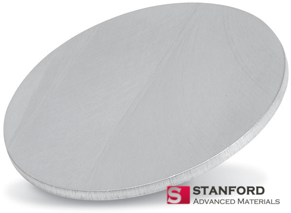
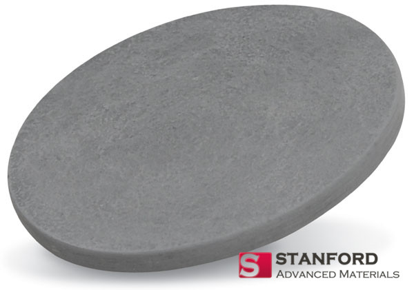
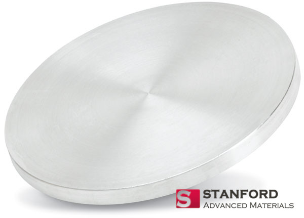
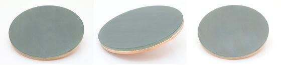
Stanford Advanced Materials (SAM) offers high-purity Niobium (Nb) Sputtering Targets engineered for demanding DC magnetron sputtering applications. With a high theoretical density of 8.57 g/cm³ and excellent thermal conductivity of 54 W/m·K, our niobium targets are the ideal choice for depositing superconducting thin films, semiconductor diffusion barriers, and advanced optical coatings. Available in purities of 99.95% and 99.99%, we can supply standard discs, plates, and fully custom shapes to meet your exact specifications.
 Niobium Sputtering Target Safety Data Sheet
High Purity Niobium (Nb) Sputtering Targets for Thin Film Deposition
| Parameter | Specification |
|---|---|
| Material | Niobium (Nb) |
| Purity | 99.95% / 99.99% |
| Appearance | Gray Metallic Surface |
| Theoretical Density | 8.57 g/cm³ |
| Melting Point | 2,468 °C |
| Thermal Conductivity | 54 W/m·K |
| Coefficient of Thermal Expansion | 7.3 x 10⁻⁶/K |
| Z-Ratio | 0.492 |
| Max Power Density | 100 W/sq. in (Recommended) |
| Available Shapes | Discs, Plates, Column Targets, Step Targets |
| Available Sizes | Diameter: 1″ – 6″ • Thickness: 0.125″ – 0.25″ |
Niobium’s unique combination of superconducting properties, chemical stability, and thermal conductivity makes it essential for advanced thin-film applications:
Superconducting Electronics:
Critical for fabricating Superconducting QUantum Interference Devices (SQUIDs) , qubits for quantum computing, and superconducting cavities for particle accelerators.
Semiconductor Manufacturing:
Used as a highly effective diffusion barrier layer in copper interconnects to prevent copper migration into silicon, ensuring device reliability. Also utilized for electrode films in advanced logic and memory chips.
Precision Optical Coatings:
Employs niobium metal layers in high-precision multilayer optical filters, laser mirrors, and DUV lithography equipment due to its durability and optical properties in the UV-VIS-NIR spectrum.
Energy Research & Storage:
Investigated for use in solid-state battery anodes, as a coating for corrosion-resistant current collectors, and in hydrogen energy systems as a hydrogen separation membrane.
Choosing the right target and process parameters is key to achieving optimal film properties.
Purity Selection:
99.95%: A cost-effective choice for general metal thin films, suitable for optical coatings, protective layers, and general R&D.
99.99%: Required for high-sensitivity applications like superconducting films, quantum devices, and semiconductor barriers where metallic impurities (e.g., Ta, W) can drastically affect performance.
Bonding Services:
While niobium has good thermal conductivity, Indium bonding to a copper backing plate is highly recommended for high-power DC magnetron sputtering. This ensures efficient heat dissipation, maintains target integrity, and prevents cracking. Explore Bonding Options →
Critical Sputtering Parameters:
Sputter Method: DC Magnetron
Z-Ratio: 0.492 – This value is essential for accurate thickness monitoring with a quartz crystal microbalance (QCM).
Power Density: To avoid target damage, it is generally recommended to stay below 100 W/sq. in.
Q: What is the Z-Ratio of a Niobium sputtering target?
A: The Z-Ratio for Niobium (Nb) is typically 0.492. This value should be entered into your film thickness monitor for accurate rate and thickness readings.
Q: What’s the difference between 99.95% and 99.99% pure niobium targets?
A: The primary difference lies in the level of trace metallic impurities (like Tantalum, Iron, Tungsten). 99.99% (4N) purity offers significantly lower impurity levels, which is critical for applications like superconductivity, where impurities disrupt the Cooper pairs, and in semiconductor junctions where they cause leakage currents.
Q: Can I order a custom size or shape not listed?
A: Absolutely. As a leading manufacturer, we specialize in custom solutions. Whether you need a specific rectangular plate, a step target, or a bonded assembly, our engineering team can fulfill your requirements. Please [Contact Us for Custom Solutions] with your drawing or specifications.
All niobium targets are vacuum-sealed and foam-padded to ensure they arrive in perfect condition, with full traceability labels.
Submit your review | |
The niobium targets were used for optical multilayer coatings in our thin-film lab. Film uniformity and adhesion were both very good, and sputtering performance was stable. I appreciate that SAM offers both indium and elastomer bonding options, which gives flexibility depending on the system setup. My only small drawback was that the lead time for custom sizes was slightly longer than expected, but the quality definitely justified it.
We’ve been using niobium sputtering targets from SAM for superconducting film deposition in our quantum device research. The purity (99.99%) has been consistent across batches, and we’ve achieved very smooth, dense coatings with no detectable contamination.
Quick delivery and good package. Perfect for film coating and sputter deposition.