| Catalog No. | ZN2277 |
|---|---|
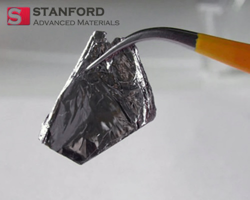
| Material | ZnO |
| Crystal Structure | Hexagonal |
| Refractive Index | 2.0681/2.0510 |
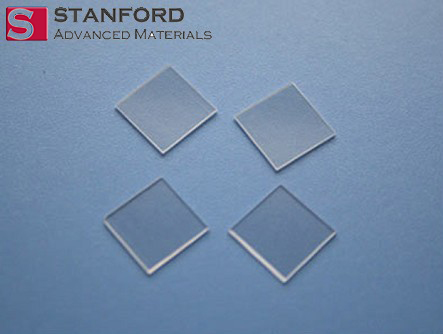
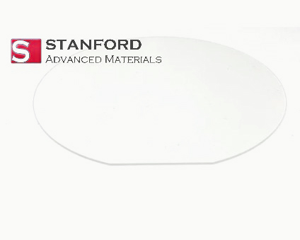
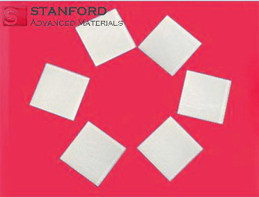
Stanford Advanced Materials (SAM) provides Zinc Oxide Wafer Substrate with size 10 x 10 x 0.5 mm. We always choose prime grade and defect-free wafer as a substrate for growing high uniformity thermal oxide layer to meet your specific requirements.
With an ideal crystal structure, the zinc oxide wafer substrate has a 2% lattice mismatch to GaN, which is much less than the lattice mismatch of the sapphire wafer and SiC wafer. ZnO wafer substrate is one of the most suitable substrates for using as GaN epitaxial growth and wide bandgap semiconductor application. ZnO wafer substrate is supplied in a square shape, undoped, size 10 x 10 x 0.5 mm, double sides polished surface finish and <0001> oriented, our high-quality ZnO wafer substrate has been widely used for the growth of nitride-based devices.
|
Chemical formula |
ZnO |
|
Crystal structure |
Hexagonal |
|
Lattice constant |
3.3 A |
|
Lattice mismatch with GaN in <0001> plane |
9 |
|
Thermal conductivity |
0.006 cal / cm /K |
|
Refractive index |
2.0681 / 2.0510 |
|
Identified polished face |
Zn-face/O-face |
Zinc oxide wafer substrates have the following applications:
– Semiconductor circuit substrate
– ZnO LED
– ZnO film
Submit your review | |