Introduction to Aluminum Nitride Semiconductor
Development of Semiconductor Materials
1 The first generation of semiconductor: represented by Si, Ge semiconductor materials;
2 The second generation of semiconductor: represented by GaAs, InP semiconductor materials;
3 The third generation of semiconductor: represented by several wide-bandgap semiconductor materials such as silicon carbide (SiC), gallium nitride (GaN), zinc oxide (ZnO), diamond, and aluminum nitride (AlN). These materials have the advantages of wide band gap, high breakdown electric field, high thermal conductivity, high electron saturation rate and high radiation resistance.
From the research and development status of the third generation semiconductor materials and devices, SiC and GaN semiconductor materials are more mature, among which SiC technology is the most mature one. Besides, research on wide-bandgap semiconductor materials such as ZnO, diamond and AlN is still in its infancy.
Further Reading: Introduction to Three Generations of Semiconductor Materials
Structure and Properties of AlN Semiconductors
Aluminum Nitride
In 1877, AlN was synthesized for the first time, but it was not until the middle of the 1980s;
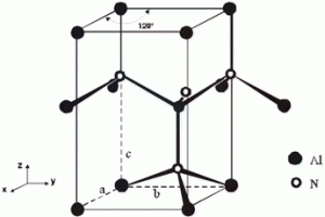
The AlN crystal has a stable hexagonal wurtzite structure with a lattice constant a=3.110 Å, c=4.978 Å;
Pure AlN crystals are colorless and transparent, but due to impurity ions and intrinsic defects present in the crystal, AlN crystals are usually yellow or amber;
According to experimental verification and theoretical calculations, AlN has the largest direct band gap width in the III-V semiconductor material, about 6.2 eV.
Various excellent performances
1 The band gap of AlN is 6.2eV, and it has a direct band gap. So it is an important blue and ultraviolet luminescent material;
2 AlN has high thermal conductivity, high resistivity, strong breakdown field and small dielectric constant. It is an excellent electronic material for high temperature, high frequency and high power devices;
3 AlN oriented along the c-axis has very good piezoelectricity and high-speed propagation of surface acoustic waves, and is an excellent piezoelectric material for surface acoustic wave devices;
4 Aluminum nitride crystal and gallium nitride crystal have very close lattice constant and thermal expansion coefficient. So AlN is the preferred substrate material for epitaxial growth of gallium nitride based optoelectronic devices.
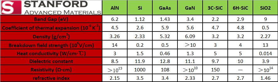
Comparison of AlN and other commonly used semiconductor materials
AlN Single Crystal Growth
Development history of AlN crystal growth
1 In 1956, Kohn et al. first grew an AlN single crystal with a diameter of 0.03 mm and a length of 0.3 mm.
2 In 1976, Slack and McNelly successfully developed AlN ingots using sublimation recondensation;
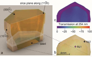
3 At present, AlN ingots larger than 2 inches in diameter have been grown in the laboratory. But there are still many needs to be resolved.
Difficulties in the growth of AlN crystals
1 AlN crystal has a very high melting point temperature (~3500K) and a large decomposition pressure. Under normal pressure conditions, AlN will decompose before melting, so it is impossible to grow AlN crystal from the melt;
2 The aluminum vapor decomposed by AlN at high temperature is very active and corrosive, and it is necessary to select a material that is resistant to high temperature and corrosion.
Methods of AlN crystal growth
1 Direct nitridation of aluminum
1) In 1960, Taylar and Lenie first used Al and N2 high-temperature reaction methods to prepare AlN single crystals, and successfully produced AlN crystal rods with a diameter of 0.5 mm and a length of 30 mm and AlN single crystal sheets with a diameter of 2 to 3 mm.
2) Schlessre et al. successfully produced an AlN single crystal wafer with an area of 50 mm2 by vaporizing metal Al in a N2 atmosphere at a reaction temperature of 2100 ° C, and the reaction lasted for 2 hrs.
2 High nitrogen pressure solution growth
When the pressure is greater than 500 MPa, the high-temperature combustion reaction rate of Al and N2 is slowed down because N2 has a higher thermal conductivity and a larger heat capacity under high pressure conditions, resulting in an increase in heat loss during the combustion reaction;
When the pressure is greater than 650 MPa, the combustion reaction is completely terminated;
In addition, the density of N2 under high pressure conditions is large, which is beneficial to reduce the evaporation and diffusion of Al;
Based on the above mechanism, Bockowski et al. successfully produced a white needle-like AlN single crystal by HNPSG method with a diameter of 1 mm and a length of 10 mm. Experimental scheme: dissolving N atom in liquid Al, wirh temperature 1800-2000K and N2 pressure 2GPa;
When the solution has a high degree of supersaturation, a wurtzite-structured AlN single crystal is obtained, but an excessively high degree of supersaturation will result in an excessively high growth rate, and an AlN single crystal having a hollow needle-like structure is easily obtained.
3 Hydride vapor phase epitaxy growth
1) Akasaki et al. first proposed the preparation of AlN single crystal by HVPE method,. The main chemical reaction equation is: AlCl3(g)+NH3(g)-AlN(g)+3HCl(g). The reaction temperature is 600-1100℃;
2) The above method is then improved: NH3 and HCl are used as reactive gases, and Ar is used as carrier gas. First, gaseous HCl reacts with metal Al to form ACI1, and then ACI3 is formed to react with NH3 to form AlN. The main chemical reaction equation: HCl ( g) +Al(l)-AlCl(g), A1Cl(g)+NH3(g)-AlN(s)+HCl(g)+H2(g).
By the above method, AlN wafers having a thickness of 75 mm and 20 mm were respectively formed on a SiC substrate and a sapphire substrate, and the diameter was 2 inches;
The advantage of the HVPE method is its fast growth rate of up to 100 mm/h, which is about 100 times that of the metal-organic gas phase deposition method and the molecular beam vapor phase epitaxy method.
4 Physical vapor transport growth
The PVT method, also known as the sublimation recondensation method, is the most successful method for growing AlN single crystals;
The reaction process: the AlN powder is first heated and sublimated at the bottom of the higher temperature crucible to become the gas phase AlN or Al and N2; then, the gas phase is transported to the top of the lower temperature crucible, and recrystallized under the N2 atmosphere to form an AlN single crystal;
Reaction temperature: The sublimation temperature of AlN is about 1800℃. But in order to obtain a large growth rate (>200mm/h) and high quality AlN single crystal, the reaction temperature must be higher than 2100℃, but lower than 2500℃. At this time, Al The vapor pressure reached 1 atm.
Requirements for crucible materials
1 The melting point is higher than 2500℃;
2 Can not form low temperature eutectic with Al, N, C, etc.;
3 Does not react with Al vapor and N2;
4 The vapor pressure is much lower than the vapor pressure of AlN formed by Al and N2;
In summary, tungsten crucible is the most ideal material for growing AlN single crystals.
Heating system
Graphite or tungsten heating elements, or microwave heating;
Using the PVT method, 2×3 mm 2 AlN flakes and needle-shaped AlN ingots having a diameter of 1 mm and a length of 3 mm were successfully produced.
Preparation of AlN Film
AlN film growth technology
1 Sputtering
N2 was used as the reaction gas, and the reaction chamber was diluted with Ar. High-purity Al sputtering target was used to form an AlN film. Parameters such as working pressure, nitrogen concentration, sputtering power, and temperature and type of the substrate have a great influence on the crystallization orientation and surface morphology of the film. Related Article: What is the sputtering target?
2 PLD
The PLD (Pulse Laser Deposition) method has the advantages of low deposition temperature, high growth rate, and maintaining the film conforming to the target composition, and is particularly suitable for multi-component compound films. There are two methods for preparing AlN films from PLD: (1) direct strip sintered AlN ceramic targets, and (2) strip pure Al targets under N2 or NH3 atmosphere.
Research Status of AlN Semiconductors (~2010)
United States
In 2002, the Semiconductor Ultraviolet Optical Sources (SUVOS) Program was launched; TDI Company of the United States is the only unit that has mastered the HVPE (Hydride Vapor Phase Epitaxy) method for preparing AlN substrate technology and realized industrialization. The AlN substrate of TDI is a 10-30 micron electrically insulating AlN layer deposited on a (0001) SiC or sapphire substrate, mainly used as a low-defect electrically insulating substrate for the fabrication of high-power AlGaN-based HEMTs. There are already 2, 3, 4, 6 inch products.
Japan
In 2004, the “High-Efficiency Ultraviolet Semiconductor” research program was launched. The best result at present is the millimeter-scale AlN single crystal, and no mature products have emerged.
China
China’s research on aluminum nitride crystals has just started. Some research institutes have also made preliminary explorations on the epitaxial growth of AlN MOCVD (metal organic vapor deposition), but there are no obvious breakthroughs and results.
Stanford Advanced Materials (SAM) Corporation is a global supplier of various sputtering targets such as metals, alloys, oxides, ceramic materials. Please visit https://www.sputtertargets.net/ for more information.
Related Product:


