Do You Know What The Anelva Target Is?
Anelva target, I believe, is a very unfamiliar phrase for most people. And maybe that’s the reason why you are here, reading this article. Actually, with a simple explanation–Anelva target is also known as the target used in the semiconductor industry, you will immediately get its meaning. In today’s semiconductor manufacturing processes, sputtering targets are undoubtedly the most important raw materials, and their quality and purity play a key role in the subsequent production quality of the semiconductor industry chain. Therefore, people created the phrase “Anelva target” to particularly indicate those targets used in semiconductor industries.
After knowing the meaning of this phrase, let’s discuss the applications of the Anelva target. In all the applications of the sputtering target, semiconductors have the highest technical requirements and purity requirements, which are significantly higher than other applications such as flat panel displays and solar cells. Thus, the price of the Anelva target is also the most expensive.
The semiconductor chipsets have extremely strict standards for the purity of the metal material and the internal microstructure of the sputtering target. If the impurity content of the sputtering target is too high, the formed film cannot achieve the required electrical properties. Moreover, it is likely to form fine particles on the wafer during the sputtering process, resulting in a short circuit or damage of the circuit, which will seriously affect the performance of the film.
Chip manufacturing has the highest requirements on the purity of the sputtering target metal, usually up to 99.9995%, and flat panel displays and solar cells just require for 99.999% and 99.995% respectively. In addition to purity, the chip also has an extremely strict requirement for the internal microstructure of the sputtering target. It is necessary to master the key technologies in the production process and practice for a long time before one can produce the products that meet the process requirements.
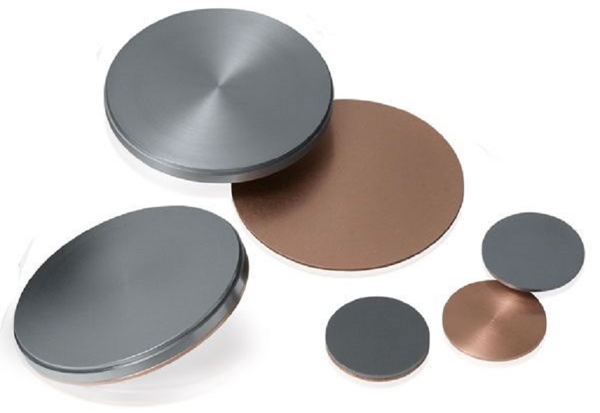
Common Anelva targets for manufacturing semiconductor chips are aluminum sputtering targets, titanium sputtering targets, tantalum sputtering targets, and so on. Common Anelva targets used in flat panel displays include molybdenum sputtering target, indium tin oxide (ITO) sputtering target, etc.
Information from SAM Sputter Target, a global sputtering target manufacturing company.


