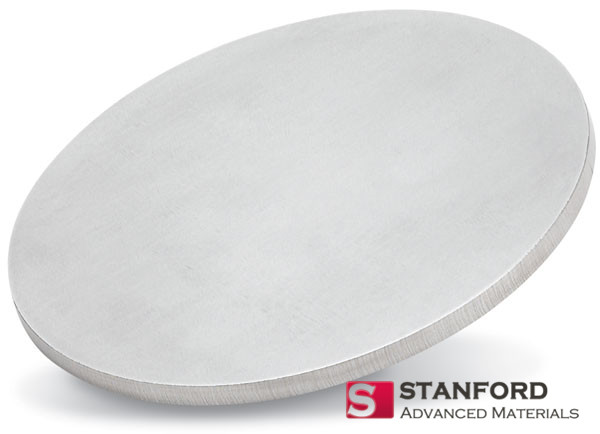
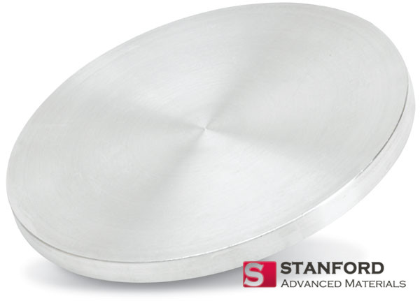
Stanford Advanced Materials (SAM) offers high-purity Molybdenum (Mo) Sputtering Targets engineered for demanding DC magnetron sputtering applications. With a density approaching 10.2 g/cm³ and exceptional thermal conductivity of 139 W/m·K, our molybdenum targets deliver smooth, hard films ideal for TFT displays, semiconductor barriers, and advanced optical coatings. Available in purities of 99.95% and 99.9%, we offer planar, rotary, and fully custom configurations to meet your exact specifications.
 Molybdenum Sputtering Target Safety Data Sheet
Molybdenum sputtering target shares properties with its source material, either pure molybdenum or molybdenum alloy. Molybdenum metal is silvery-white and very hard. Its melting point is 2623°C (4753°F), which is only lower than tantalum, osmium, rhenium, tungsten among natural elements. It also has one of the lowest coefficients of thermal expansion among metals in commercial use.
Molybdenum target has a density of almost 100 %. The denser the Mo target is, the better the conductivity of the created layer. SAM specializes in producing high purity sputtering target materials with the highest possible density and smallest possible average grain sizes for use in the PVD, CVD, APS and VPS coating processes. You benefit from a faster process due to higher sputtering speeds.
| Parameter | Specification |
|---|---|
| Material Type | Molybdenum (Mo) |
| Symbol | Mo |
| Atomic Weight | 95.96 |
| Atomic Number | 42 |
| Color/Appearance | Grey, Metallic |
| Theoretical Density | 10.2 g/cm³ (10,200 kg/m³) |
| Melting Point | 2,617 °C (4,743 °F) |
| Thermal Conductivity | 139 W/m·K |
| Coefficient of Thermal Expansion | 4.8 x 10⁻⁶/K |
| Z Ratio | 0.257 |
| Sputter Method | DC |
| Max Power Density (Unbonded) | 150 W/sq.in * |
| Max Power Density (Bonded) | ≤ 20 W/sq.in * |
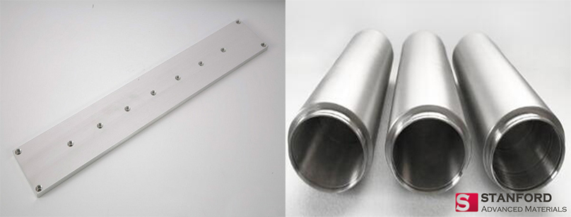
| Available Shapes | Discs (Planar), Rotary, Plates, Step Targets |
| Standard Sizes | Dia.: 1.0″, 2.0″, 3.0″, 4.0″, 5.0″, 6.0″ • Thick: 0.125″, 0.250″ |
| Comments | Films smooth, hard. Careful degas required. |
*Note: Power density recommendations are based on optimal thermal contact and sputter-up orientation. Bonded targets require significant power reduction to prevent bond failure. Contact our engineers for specific process guidance.
Molybdenum’s unique combination of high melting point, low thermal expansion, and excellent electrical conductivity makes it essential for advanced thin-film applications:
Flat Panel Displays & TFT-LCD:
Widely used as an electrode material and diffusion barrier in thin-film transistor (TFT) liquid crystal displays due to its good conductivity and etchability.
Semiconductor Manufacturing:
Serves as a gate metal in MOSFET devices and as a barrier layer in interconnect structures to prevent metal diffusion.
Thin-Film Solar Cells:
Commonly used as the back contact electrode in CIGS (Copper Indium Gallium Selenide) thin-film solar cells due to its high conductivity and reflectivity.
X-Ray Optics:
A critical component in mammography X-ray tubes and multilayer mirrors for X-ray fluorescence (XRF) analysis.
Optical Coatings:
Used in multilayer optical stacks for high-reflectivity mirrors and beam splitters in the UV-VIS-NIR spectrum.
Achieving optimal film quality requires careful selection of target specifications and process parameters.
Purity Selection:
99.9%: Suitable for general metal coatings, decorative applications, and non-critical R&D.
99.95%: Required for high-performance applications like TFT-LCD electrodes, semiconductor barriers, and CIGS solar cells where trace impurities can significantly impact device performance and yield.
Bonding & Power Management:
Critical Warning: While Indium bonding to a copper backing plate is highly recommended for high-power applications to ensure efficient heat dissipation, bonded targets must be run at significantly lower power densities (≤ 20 W/sq.in) than unbonded targets to prevent bond line failure.
For unbonded targets, ensure excellent thermal contact with the cathode cooling system. Thermal paste may be required for optimal heat transfer.
Rotary vs. Planar Targets:
Rotary (Rotatable) Targets: Offer >75% material utilization, making them cost-effective for high-volume production runs in large-area coating (architectural glass, displays).
Planar Targets: Ideal for R&D, pilot production, and applications with smaller substrate sizes. Available in single-piece or multi-piece configurations.
Q: What is the Z-Ratio of a Molybdenum sputtering target?
A: The Z-Ratio for Molybdenum (Mo) is typically 0.257. This value should be entered into your quartz crystal microbalance (QCM) for accurate film thickness monitoring.
Q: Why is molybdenum used in CIGS solar cells?
A: Molybdenum is the material of choice for the back contact in CIGS solar cells because it forms a low-resistance ohmic contact with the CIGS absorber layer, has high thermal stability during processing, and reflects unabsorbed light back through the absorber.
Q: What is the difference between 99.9% and 99.95% pure molybdenum targets?
A: The 99.95% purity grade has significantly lower levels of trace metallic impurities (such as Fe, Ni, Cr). This higher purity is essential for semiconductor and display applications where metallic contamination can cause electrical leakage, recombination centers, or visual defects.
Q: Can I operate a bonded molybdenum target at high power?
A: No. Bonded targets (typically with indium) have a maximum recommended power density of ≤ 20 W/sq.in. Exceeding this can melt the indium bond, causing catastrophic target delamination and system contamination. Unbonded targets can handle up to 150 W/sq.in with proper thermal management.
Q: Can you provide custom sizes or bonded assemblies?
A: Absolutely. As a leading manufacturer, we specialize in custom solutions. We can provide targets in custom dimensions and bond them to your specified backing plate material (copper, molybdenum, stainless steel). Please [Contact Us for Custom Solutions] with your requirements.
Our molybdenum sputter targets are carefully handled to prevent damage during storage and transportation and to preserve the quality of our products in their original condition.
SAM’s molybdenum sputtering targets are available in various forms, purities, sizes, and prices. We specialize in producing high purity thin film coating materials with the highest possible density and smallest possible average grain sizes for use in semiconductor, chemical vapor deposition (CVD) and physical vapor deposition (PVD) display and optical applications. Please send us an inquiry for the current prices of sputtering targets and other deposition materials that are not listed.
Submit your review | |
I bought a 1" Molybdenum target for a small-scale research project. It was exactly what I needed, and the results were outstanding. The quality of the films produced exceeded my expectations. Highly recommended for experimental setups!
Just received a 3" Mo sputtering target with a thickness of 0.25". The delivery was prompt and the target performed exceptionally well in my thin-film solar cell experiments. It's great to have such reliable materials for my research!
I got exactly what I wanted to receive. Exact size as advertised. There are too many options of sizes. Will buy it again.