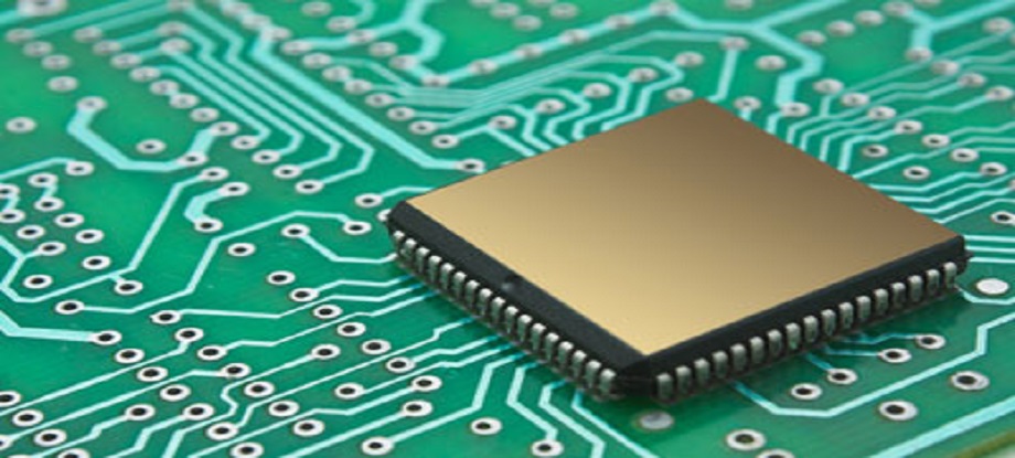
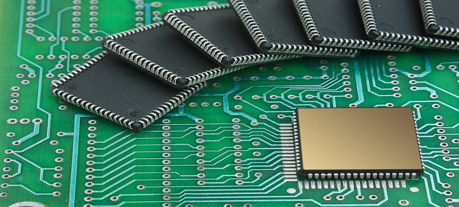
Stanford Advanced Materials (SAM) is your advanced materials partner for the semiconductor industry. We supply ultra-high purity (99.99% to 99.99999%) compound semiconductor materials and mission-critical PVD sputtering targets engineered to meet the challenges of next-generation fabrication.
Our expertise helps you tackle key issues in thin film deposition—from enabling sub-3nm logic interconnects and ensuring step coverage in 3D NAND to optimizing the total cost of ownership (TCO) for your process.
Jump directly to the materials and insights for your specific challenge.
The Challenge: As device scaling continues, traditional barrier/liner materials for Cu interconnects face fundamental limits in resistivity and gap-fill capability within increasingly confined spaces.
Key Materials & Focus: Cobalt (Co) Targets for low-resistivity barriers and Ruthenium (Ru) Targets as an ideal liner for direct Cu plating. Performance hinges on ultra-high purity and precise grain structure control.
Deep Dive: Compare Co vs. Ru performance data, understand process integration for FinFET/GAA structures, and learn the 5 critical questions to ask your target supplier.
The Challenge: Optimizing the process window for DRAM capacitor electrodes and achieving conformal step coverage in the extreme aspect-ratio structures of 3D NAND.
Key Materials & Focus: Aluminum (Al) and Titanium Nitride (TiN) Targets for DRAM capacitors; Tantalum (Ta) and Tantalum Nitride (TaN) Targets for robust barrier layers in 3D NAND.
Deep Dive: Analyze material selection strategies, cost implications of increasing stack layers, and the balance between PVD and emerging techniques like ALD.
The Challenge: High cost of 300mm targets, productivity loss from low utilization rates, and unplanned downtime due to target failure.
The Solution: Advanced target design (rotary vs. planar, asymmetric) and superior bonding technology (brazing, soldering) to extend target life and improve thermal management.
Deep Dive: Learn how design and bonding innovations can boost utilization by 30% or more, and access a model to calculate the true ROI of your targets.
Our most critical materials for advanced semiconductor fabrication, available in ultra-high purity grades and customized forms including sputtering targets.