(949) 407-8904 Mon - Fri 08:00 - 17:00 1940 East Deere Avenue, Suite 100, Santa Ana, CA 92705, USA

Company Dynamic

Cost Reduction Path for Large-Size OLED Electrodes: ITO Optimization, Silver Alloys & New TCOs

Abstract: As OLED displays scale to larger formats, the cost of the transparent electrode becomes a critical bottleneck. This article maps the practical engineering strategies for cost reduction across three material fronts: pushing incumbent ITO to its efficiency limits, integrating novel silver alloy anodes, and evaluating the readiness of next-generation TCO alternatives. We provide a decision...
Continue Reading

An Overview of Magnetron Sputtering

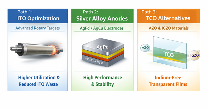
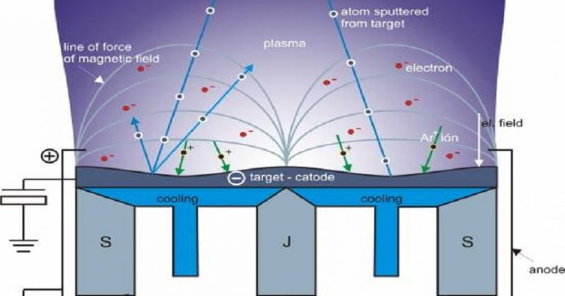
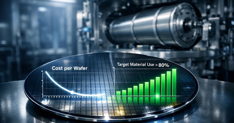
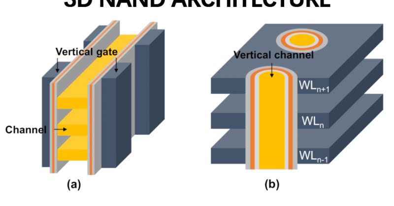
An Overview of Magnetron Sputtering Magnetron sputtering, a physical vapor deposition (PVD) process, is a main thin film deposition method for manufacturing semiconductors, disk drives, CDs, and optical devices. Magnetron sputtering has the advantages of high speed, low temperature, and low damage. In this article, let’s take a look at the definition, working principle, and...
Continue Reading
optimize-target-tco

Semiconductor Target TCO Analysis: Boosting Utilization by 30% via Design & Bonding

Abstract: In semiconductor manufacturing, the cost of a PVD sputtering target extends far beyond its purchase price. For 300mm targets, low utilization rates and unscheduled downtime due to bonding failures represent massive, hidden costs. This article provides a Total Cost of Ownership framework, demonstrating how strategic target design (rotary vs. planar, asymmetric erosion profiles) and advanced...
Continue Reading
Platinum vs. Gold Ring

Should You Choose Platinum or Gold for Your Wedding Ring in 2026?

Back in 2019, we published a guide comparing platinum and gold rings. It quickly became one of our most-read articles, helping readers make informed choices about their wedding jewelry. But times have changed — and so have the reasons behind choosing one metal over the other. If you’re shopping in 2026, here’s what actually matters....
Continue Reading
3D-NAND-COVER

PVD Targets for DRAM & 3D NAND Manufacturing: From Capacitor Electrodes to Step Coverage

Abstract: The divergence in memory architecture between DRAM and 3D NAND Flash presents unique thin-film deposition challenges, directly impacting cost and performance. This article dissects the critical PVD target strategies for both technologies: the pursuit of seamless, high-aspect-ratio fill for DRAM capacitors, and the battle for conformal step coverage in 3D NAND’s towering staircases. We...
Continue Reading
3nm 2nm chips

Key PVD Target Guide for 3nm/2nm Nodes: Selecting Cobalt & Ruthenium Barrier Layers

As the semiconductor industry advances beyond the 5nm node, conventional barrier/liner materials, such as Ta/TaN, are approaching their physical limits. This article provides a technical point of view of the two most promising successors: Cobalt (Co) and Ruthenium (Ru) PVD targets. We compare their material properties, process integration challenges, and selection criteria for advanced FinFET and...
Continue Reading
1 2 3 4 49