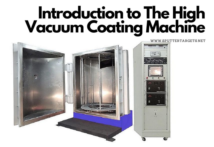
In this post, you are going to learn What is vaccum coating? The structure of the high vacuum coating machine Basic technical requirements for high vacuum coating equipment The use of the high vacuum coating machine Features of high vacuum coating equipment What is Vaccum Coating? Vacuum coating is a thin-film technology to deposit thin films...Continue Reading
1. What types of coating technology can be divided into? (1) Vacuum coating (2) Electroplating (3) Chemical reaction (4) Heat treatment (5) Physical or mechanical treatment 2. What are the applications of plasma technology in surface technology? Sputter deposition: Sputtering is the use of high-speed ions to strike a solid sputter target, causing surface molecules...Continue Reading
AlxCr1-xN coatings have excellent mechanical properties and oxidation resistance and are therefore of high application value in a variety of industrial applications. In recent years, the effects of various deposition parameters (such as partial pressure, gas mixture or temperature) on the sputtering process have been studied, but there has been little research on the influence...Continue Reading
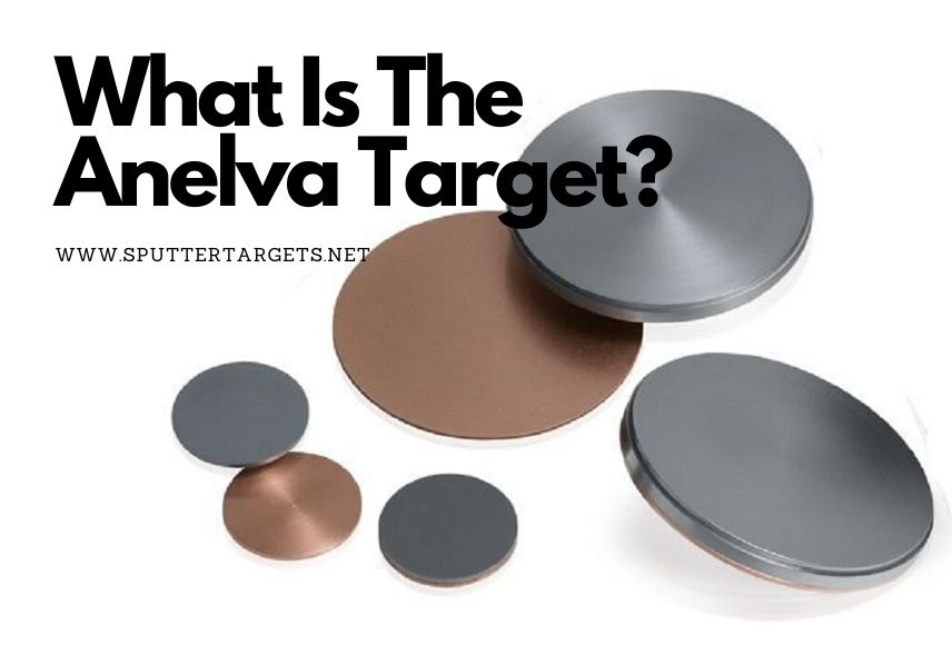
Anelva target, I believe, is a very unfamiliar phrase for most people. And maybe that’s the reason why you are here, reading this article. Actually, with a simple explanation–Anelva target is also known as the target used in the semiconductor industry, you will immediately get its meaning. In today’s semiconductor manufacturing processes, sputtering targets are...Continue Reading
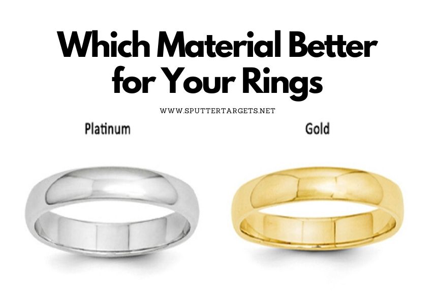
As for the two most commonly used metals for engagement and wedding rings, platinum and gold, most people distinguish them by their different colors-platinum is naturally white, and gold is naturally yellow. However, rings made of white gold (composed of gold, alloys, and a rhodium plating) have a similar white color to platinum rings. Since...Continue Reading
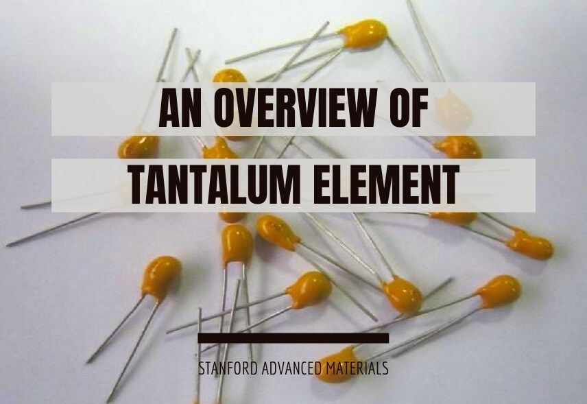
Tantalum Overview The texture of the tantalum is very hard and the hardness can reach 6-6.5. Its melting point is as high as 2996 °C, only after carbon, tungsten, rhenium, and osmium. Tantalum is malleable and can be drawn into a thin foil. Its coefficient of thermal expansion is very small, and it only expands by 6.6 parts...Continue Reading
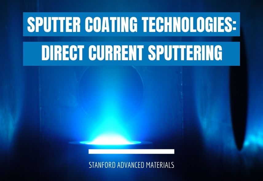
We have previously made a brief introduction of Five Sputter Coating Technologies, including unbalanced magnetron sputtering, radio frequency sputtering (RF sputtering), direct current magnetron sputtering (DC sputtering), mid-frequency alternating current magnetron sputtering (AC sputtering), and reactive magnetron sputtering. In this article, we are going to talk about direct current (DC) sputtering in detail. To begin...Continue Reading
Sputtering targets have important applications in many areas, such as architecture, optics, electronics and so on. Sputtering targets used in electronic industry can be subdivided into semiconductor target (also called anelva target), planar target, coated glass target, solar photovoltaic target, and so on. There are some differences in the selection and performance requirements of sputtering materials in different application fields....Continue Reading
Sputtering targets are a physical vapor deposition (PVD) mechanism with many uses in modern technology and manufacturing. In the sputtering process, the atoms are pulled from the sputter target with powerful magnets, and a controlled gas (usually argon) is introduced. Then, the processed to collide with each other in their gaseous state before condensing into...Continue Reading