Home
Product
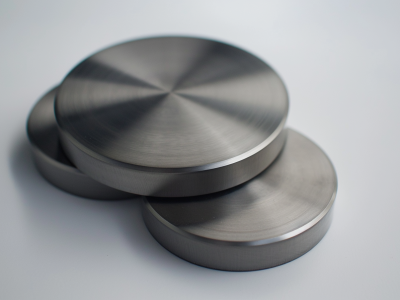
Sputtering Target
By Chemical Elements
Evaporation Materials
By Evaporation Materials
By Chemical Elements
Bonding Service
Indium Target Bonding Service
OFHC Copper Backing Plates
Elastomeric Target Bonding Service
Planar Targets
Evaporation Sources
Thermal sources
E-Beam Source Used Crucibles
3D Printing Powder
Crystal Substrates
Thermal Spraying Coating
Application
Architectural, Automotive Glass & WEB Coating
Semiconductor Materials
Hardware & Decorative Coatings
Optics Coatings
Solar
Electronics
FAQ
About Us
NEWS
Blogs
Industry News
Most Popular
Contact Us
(949) 407-8904
Mon - Fri 08:00 - 17:00
1940 East Deere Avenue, Suite 100, Santa Ana, CA 92705, USA
Get A Quote
Home
Products
Sputtering Targets
By Material Types
By Chemical Elements
Evaporation Materials
By Material Types
By Chemical Elements
Precious Metals
Gold Sputtering Target
Silver Sputtering Target
Platinum Sputtering Target
Gold Evaporation Materials
Evaporation Source
Thermal Sources
Alumina Boat
E-Beam Source Used Crucibles
Graphite Crucible
Tungsten Crucible
Boron Nitride Crucible
Zirconia Crucible
Crystal Substrates
Calcium Carbonate Crystal
Barium Titanate Crystal
Rutile Titanium Dioxide Crystal
3D Printing Powders
Thermal Spraying Coating
Targets
By Target Shapes
Planar Sputtering Target
Rotary Sputter Target
Rare Earth Targets
Erbium Sputtering Target
Praseodymium Sputtering Target
Pure Metal Targets
Gold Sputtering Target
Iridium Sputtering Target
Aluminum Target
Alloy Targets
Ti/W Sputtering Target
Mo/Nb Alloy Rotary Target
Nb/Ti Sputtering Target
Oxide Targets
SiO2 Sputtering Target
Magnesium Oxide Target
Aluminum Oxide Sputtering Target
Nitride Targets
TiN Sputtering Target
AlN Sputtering Target
Boron Nitride Sputtering Target
Fluoride Targets
MgF2 Sputtering Target
LiF Sputtering Target
Carbide Targets
Silicon Carbide Sputtering Target
Fe3C Sputtering Target
Pellets
Pure Metal Pellets
Gold Evaporation Materials
Alloy Pellets
Oxide Pellets
Nitride Pellets
Niobium Nitride Evaporation Materials
Fluoride Pellets
Magnesium Fluoride Evaporation Materials
Carbide Pellets
Iron Carbide Evaporation Materials
Silicide Pellets
Sulfide Pellets
Boride Pellets
Selenide Pellets
Services
Target Bonding
Indium Bonding
Copper Backing Plates
Elastomeric Bonding Service
Target Recycling
Applications
Solar
CIGS Sputtering Target
Semiconductors
Electronics
Lithium Niobate Sputtering Target
Optics Coatings
Hardware & Decorative Coatings
Automotive Glass & WEB Coating
About
Blogs
Cornerstone Articles
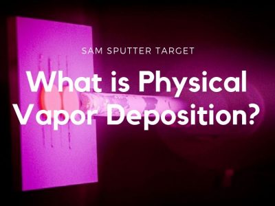
What is Physical Vapor Deposition (PVD)?
What is Chemical Vapor Deposition (CVD)? The Ultimate Guide
Glossary
Terms & Conditions
MSDS Listings
Privacy Policy
Friend Links
FAQ
Inquiry
Category
Blog
August 15, 2025
Julissa Green
Blog
,
Specific Materials
High-Purity Niobium Sputtering Targets in Semiconductor Chip Fabrication
Introduction Thin film deposition is an integral part of semiconductor chip production. Sputtering is perhaps...
July 31, 2025
Julissa Green
Blog
Zirconium Sputtering Targets in Semiconductor Chip Manufacturing
Introduction The semiconductor industry is driving the technological revolution, fueling the progress of electronics, computing, and communications. As performance demands rise and chip dimensions continue to be reduced, the material employed...
July 24, 2025
Julissa Green
Applications
,
Blog
Case Study: Improving ITO Target Performance in Mobile and Tablet Display Manufacturing
Introduction One of SAM’s long-term clients—a major display panel manufacturer—was experiencing frequent production disruptions. The...
July 17, 2025
Julissa Green
Blog
Chromium Sputter Targets’ Value in Semiconductor Manufacturing
Introduction The semiconductor industry is the backbone of modern-day technology, powering everything from smartphones to...
July 10, 2025
Julissa Green
Blog
High-Purity Vanadium Sputtering Targets in Semiconductor Applications
In the semiconductor industry, the demand for smaller, faster, and lower power devices has created...
July 7, 2025
Julissa Green
Blog
,
Cornerstone
,
Most Popular
What is Physical Vapor Deposition (PVD)?
What is PVD Coating Technology? Physical Vapor Deposition (PVD) is a thin film preparation technique...
July 3, 2025
Julissa Green
Blog
Tantalum Sputtering Targets in Semiconductor Manufacturing
The insatiable requirement for thinner, faster, and power-saving technologies has made the semiconductor industry one...
June 26, 2025
Julissa Green
Blog
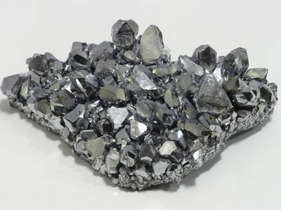
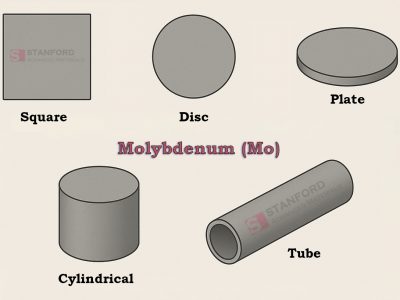
Molybdenum Targets: Classification by Shapes and Applications
In thin film technology, materials need more than just potential—they need consistency, resilience, and performance...
June 4, 2025
Julissa Green
Blog
Choosing Powder Metallurgy for High-Performance Sputtering Targets
1. Introduction Sputtering targets play a central role in physical vapor deposition (PVD) processes, forming...
1
…
3
4
5
6
7
…
33
Product categories
Sputtering Target
Alloy Targets
By Chemical Elements
Ceramic Targets
Other Compound Targets
Pure Metal Targets
Advanced Materials
3D Printing Powder
Crystals & Substrates
Specialty Wires & Foils
Thermal Spraying Coating
Bonding Service
Elastomeric Target Bonding Service
Indium Target Bonding Service
OFHC Copper Backing Plates
Evaporation Materials
Alloy Evaporation Materials
By Chemical Elements
By Evaporation Materials
Ceramic Evaporation Materials
Metal
Evaporation Sources
E-Beam Source Used Crucibles
Thermal sources
Featured Products
ST0033 Niobium Sputtering Target, Nb
ST6843 Silicon (Si) Rotary Sputtering Target
ST11173 Sodium Phosphate (Na3PO4) Sputtering Target
ST11221 Zinc Sulfide (ZnS) Planar Sputtering Target
ST11220 Zinc (Zn) Rotary Sputtering Target