Home
Product
Sputtering Target
By Chemical Elements
Evaporation Materials
By Evaporation Materials
By Chemical Elements
Bonding Service
Indium Target Bonding Service
OFHC Copper Backing Plates
Elastomeric Target Bonding Service
Planar Targets
Evaporation Sources
Thermal sources
E-Beam Source Used Crucibles
3D Printing Powder
Crystal Substrates
Thermal Spraying Coating
Application
Architectural, Automotive Glass & WEB Coating
Semiconductor Materials
Hardware & Decorative Coatings
Optics Coatings
Solar
Electronics
FAQ
About Us
NEWS
Blogs
Industry News
Most Popular
Contact Us
(949) 407-8904
Mon - Fri 08:00 - 17:00
1940 East Deere Avenue, Suite 100, Santa Ana, CA 92705, USA
Get A Quote
Home
Products
Sputtering Targets
By Material Types
By Chemical Elements
Evaporation Materials
By Material Types
By Chemical Elements
Precious Metals
Gold Sputtering Target
Silver Sputtering Target
Platinum Sputtering Target
Gold Evaporation Materials
Evaporation Source
Thermal Sources
Alumina Boat
E-Beam Source Used Crucibles
Graphite Crucible
Tungsten Crucible
Boron Nitride Crucible
Zirconia Crucible
Crystal Substrates
Calcium Carbonate Crystal
Barium Titanate Crystal
Rutile Titanium Dioxide Crystal
3D Printing Powders
Thermal Spraying Coating
Targets
By Target Shapes
Planar Sputtering Target
Rotary Sputter Target
Rare Earth Targets
Erbium Sputtering Target
Praseodymium Sputtering Target
Pure Metal Targets
Gold Sputtering Target
Iridium Sputtering Target
Aluminum Target
Alloy Targets
Ti/W Sputtering Target
Mo/Nb Alloy Rotary Target
Nb/Ti Sputtering Target
Oxide Targets
SiO2 Sputtering Target
Magnesium Oxide Target
Aluminum Oxide Sputtering Target
Nitride Targets
TiN Sputtering Target
AlN Sputtering Target
Boron Nitride Sputtering Target
Fluoride Targets
MgF2 Sputtering Target
LiF Sputtering Target
Carbide Targets
Silicon Carbide Sputtering Target
Fe3C Sputtering Target
Pellets
Pure Metal Pellets
Gold Evaporation Materials
Alloy Pellets
Oxide Pellets
Nitride Pellets
Niobium Nitride Evaporation Materials
Fluoride Pellets
Magnesium Fluoride Evaporation Materials
Carbide Pellets
Iron Carbide Evaporation Materials
Silicide Pellets
Sulfide Pellets
Boride Pellets
Selenide Pellets
Services
Target Bonding
Indium Bonding
Copper Backing Plates
Elastomeric Bonding Service
Target Recycling
Applications
Solar
CIGS Sputtering Target
Semiconductors
Electronics
Lithium Niobate Sputtering Target
Optics Coatings
Hardware & Decorative Coatings
Automotive Glass & WEB Coating
About
Blogs
Cornerstone Articles
What is Physical Vapor Deposition (PVD)?
What is Chemical Vapor Deposition (CVD)? The Ultimate Guide
Glossary
Terms & Conditions
MSDS Listings
Privacy Policy
Friend Links
FAQ
Inquiry
Category
Most Popular
January 15, 2026
Julissa Green
Blog
,
Cornerstone
,
Information
,
Most Popular
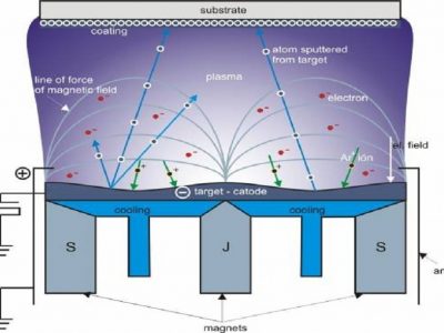
An Overview of Magnetron Sputtering
An Overview of Magnetron Sputtering Magnetron sputtering, a physical vapor deposition (PVD) process, is a...
December 16, 2025
Julissa Green
Applications
,
Blog
,
Information
,
Most Popular
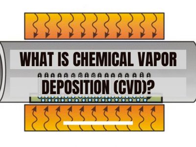
What is Chemical Vapor Deposition (CVD)? The Ultimate Guide
Introduction Chemical Vapor Deposition (CVD) might sound like an obscure lab technique, but it’s the...
October 30, 2025
Julissa Green
Blog
,
Cornerstone
,
Most Popular
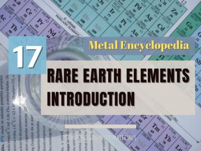
Metal Encyclopedia: Seventeen Rare Earth Elements Introduction
Rare-earth element is a general term for 17 elements of lanthanides as well as scandium...
October 13, 2025
Julissa Green
Applications
,
Blog
,
Most Popular
,
Specific Materials
6 Crucial Aluminum Uses in Daily Life (And Why It’s Everywhere)
Aluminum is everywhere. Cars, foil, power lines, window frames — you name it. It’s lightweight,...
October 10, 2025
Julissa Green
Applications
,
Blog
,
Comparison
,
Most Popular
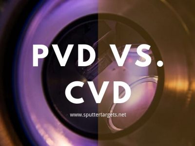
Table Comparison: Physical Vapor Deposition Vs. Chemical Vapor Deposition
1. The Core Difference at a Glance Before diving deep, here is the fundamental distinction:...
September 10, 2025
Julissa Green
Applications
,
Blog
,
Cornerstone
,
Most Popular
,
Specific Materials
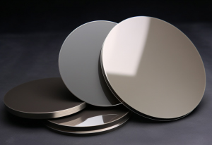
Everything You Need to Know About Sputtering Targets
1. Introduction to Sputtering Targets Sputtering targets are significant commodities for thin-film industries like electronics,...
July 7, 2025
Julissa Green
Blog
,
Cornerstone
,
Most Popular
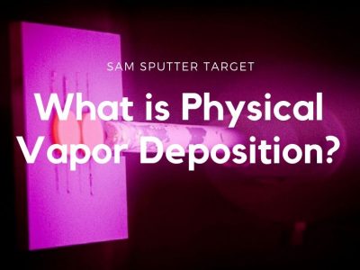
What is Physical Vapor Deposition (PVD)?
What is PVD Coating Technology? Physical Vapor Deposition (PVD) is a thin film preparation technique...
May 6, 2025
Julissa Green
Blog
,
Most Popular
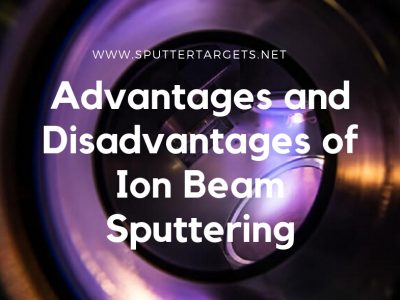
Advantages and Disadvantages of Ion Beam Sputtering
Ion Beam Sputtering Definition Ion beam sputtering (IBS), or ion beam deposition (IBD), is a thin...
April 2, 2025
Julissa Green
Blog
,
Most Popular
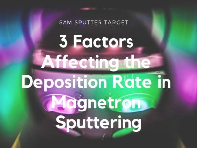
3 Factors Affecting the Deposition Rate in Magnetron Sputtering
Magnetron sputtering is a physical vapor deposition method that allows the deposition of various materials,...
1
2
3
…
5
Product categories
Sputtering Target
Alloy Targets
By Chemical Elements
Ceramic Targets
Other Compound Targets
Pure Metal Targets
Advanced Materials
3D Printing Powder
Crystals & Substrates
Specialty Wires & Foils
Thermal Spraying Coating
Bonding Service
Elastomeric Target Bonding Service
Indium Target Bonding Service
OFHC Copper Backing Plates
Evaporation Materials
Alloy Evaporation Materials
By Chemical Elements
By Evaporation Materials
Ceramic Evaporation Materials
Metal
Evaporation Sources
E-Beam Source Used Crucibles
Thermal sources
Featured Products
ST0033 Niobium Sputtering Target, Nb
ST6843 Silicon (Si) Rotary Sputtering Target
ST11173 Sodium Phosphate (Na3PO4) Sputtering Target
ST11221 Zinc Sulfide (ZnS) Planar Sputtering Target
ST11220 Zinc (Zn) Rotary Sputtering Target