Table Comparison: Physical Vapor Deposition Vs. Chemical Vapor Deposition
1. The Core Difference at a Glance
Before diving deep, here is the fundamental distinction:
-
PVD (Physical Vapor Deposition): A physical process. A solid material is vaporized in a vacuum and then condenses as a thin film on the substrate. Think of it as transferring material atom-by-atom.
-
CVD (Chemical Vapor Deposition): A chemical process. Gaseous precursors react or decompose on the heated substrate surface, forming a solid coating. Think of it as “growing” a coating from a chemical reaction.
2. Technical Comparison Table
| Feature | Physical Vapor Deposition (PVD) | Chemical Vapor Deposition (CVD) |
|---|---|---|
| Process Type | Physical transformation (solid → vapor → solid) | Chemical reaction on the substrate surface |
| Typical Techniques | Sputtering: Using plasma to eject atoms from a target. Evaporation: Using high heat to vaporize a source material. |
LPCVD, PECVD, MOCVD |
| Applications | Microelectronics, solar panels, optical coatings, cutting tools | Semiconductor fabrication, diffusion barriers, wear-resistant coatings |
| Deposition Temperature | Relatively low (<500°C) | High (typically >900°C), may affect substrate properties |
| Coating Uniformity | Poor on complex surfaces; prone to shadowing | Excellent; coats internal features and complex geometries |
| Film Thickness | ~2.5 μm | ~7.5 μm |
| Surface Finish | Smooth, metallic luster, replicates substrate finish | Slightly rougher; may require post-processing |
| Pre-cleaning Requirements | High; requires very clean surfaces | Lower sensitivity to surface cleanliness |
| Environmental Impact | Low; considered a clean, “green” technology | Can involve hazardous gases and byproducts |
| Cost | Generally more expensive due to equipment and vacuum needs | More cost-effective for high-volume production |
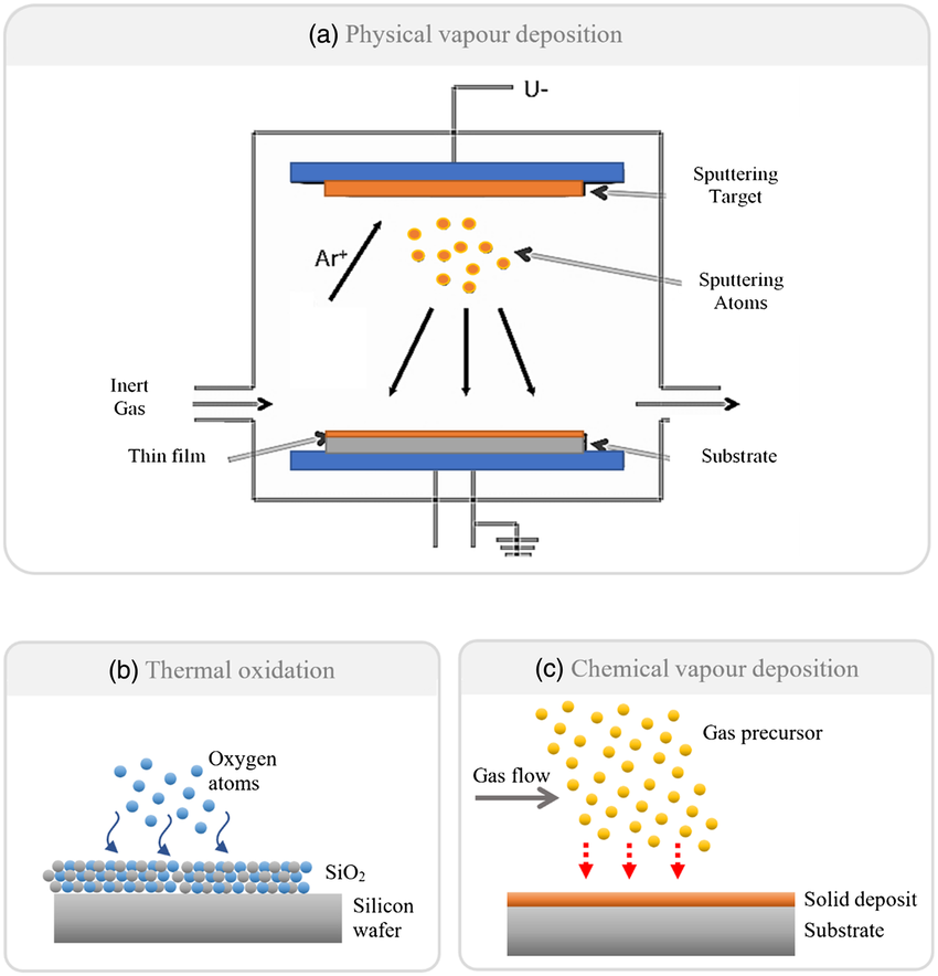
3. Visual Comparison: PVD vs. CVD at a Glance
4. Industry Applications: Use Case Breakdown
1. Semiconductor Manufacturing
- CVD is preferred for oxide/nitride layers and materials like tungsten, offering excellent conformity.
- PVD is used for metal interconnects like copper and aluminum, requiring high purity and thickness control.
2. Cutting Tools and Molds
- PVD is ideal for HSS Tools: Its low temperature preserves the tool’s hardness, applying a hard, thin, and wear-resistant coating like TiN.
- CVD fits Carbide Tools: It builds thicker coatings with superior wear resistance (e.g., Al₂O₃), though the high temperature may require subsequent heat treatment.
3. Aerospace & Automotive
- CVD enables ceramic coatings (SiC, TiC) for thermal and corrosion resistance.
- PVD supports IR windows, decorative layers like gold-tone TiN and optical Al2O3 layers.
4. Optics and Displays
- PVD is a go-to for mirrors, AR/IR coatings, and OLED protection.
- CVD applies conductive or hydrophobic layers with specific chemical functionality.
5. Clean Energy (Solar, Fuel Cells)
- PVD is used for ITO transparent conductive films in thin-film solar tech.
- CVD is used for polysilicon layers, CNT growth, and structural coatings.
5. How to Choose: Practical Recommendations
| Scenario | Recommended Method | Reasoning |
|---|---|---|
| High-temperature carbide tools | CVD | Thicker, more wear-resistant coatings |
| Optical glass or decorative coatings | PVD | Superior aesthetics, adhesion, and low temp |
| Semiconductor metal interconnects | PVD | High purity and precise thickness control |
| Parts with complex 3D geometries | CVD | Unmatched conformal coverage without shadowing |
| Temperature-sensitive substrates | PVD | Low process temperature prevents damage |
6. Conclusion & Next Steps
Both PVD and CVD are powerful techniques with distinct advantages. PVD excels in low-temperature applications requiring high purity and specific metallurgical properties, while CVD is unmatched for coating complex shapes with uniform, high-performance layers at high temperatures.
Ready to Specify Your Thin-Film Solution?
This comparison is just the beginning. When you’re ready to select the ideal coating for your specific application, the experts at Stanford Advanced Materials (SAM) are here to help.
We provide:
- High-Purity Materials: A wide range of sputtering targets, evaporation sources, and CVD precursors.
- Technical Consultation: Expert guidance to help you choose the right material and process for your project.
- Custom Fabrication: Tailored solutions to meet your unique specifications.
Contact Stanford Advanced Materials (SAM) today to discuss your project requirements and request a quote.
References
-
Selvakumar, N., & Barshilia, H. C. (2012). Review of physical vapor deposited (PVD) spectrally selective coatings for mid- and high-temperature solar thermal applications. Solar Energy Materials and Solar Cells.
-
Musbah, A., et al. (2022). Comparison Between Chemical Vapor Deposition CVD and Physical Vapor Deposition PVD Coating Techniques: A Review Paper.
- Hassanin, Hany & Sheikholeslami, Ghazal & Sareh, Pooya & Ishaq, Rihana. (2021). Microadditive Manufacturing Technologies of 3D Microelectromechanical Systems. Advanced Engineering Materials. 23. 10.1002/adem.202100422.


