Everything You Need to Know About Niobium Sputtering Targets for High-Performance Applications
Introduction
In the field of material science and thin-film deposition, many industries rely on precise methods to create films on surfaces. Electronics, aerospace, and solar energy all need reliable coatings to work properly. One important material used in these processes is the niobium sputtering target.
Sputtering is a process where atoms are ejected from a material and then deposited onto a substrate. This method forms thin and even films. Niobium stands out because it has a high melting point, resists corrosion well, and conducts electricity efficiently. These qualities are very important for demanding industrial applications.
Definition and Overview of the Niobium Sputtering Target
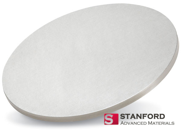
Simply put, a niobium sputtering target is a piece of pure niobium specially prepared for the sputtering process. It starts as refined niobium metal that is shaped and tested for quality. The metal itself is a shiny, silver-gray element found in the earth’s crust, though in very small amounts (around 20 parts per million). When used in sputtering, the niobium target releases niobium atoms. These atoms land on a nearby surface and create a thin film that can serve as a conductive layer in electronic parts or act as a protective coating.
Properties of Niobium and Its Role in Thin-Film Deposition
Niobium is well known among engineers and scientists for its consistent and useful properties. Let us consider some key points:
• High melting point: Niobium melts at around 2,468 °C. This means it handles very high temperatures without losing its structure. In processes where heat is a factor, such as in aircraft engines or high-power electronics, this is a critical advantage.
• Corrosion resistance: When exposed to air, niobium quickly forms a stable oxide layer. This natural film protects the metal from further corrosion. In industries where chemical exposure or extreme weather is a risk, this resistance is very helpful.
• Electrical conductivity: Niobium is an excellent conductor of electricity. It is often used in making capacitors, transistors, and other electronic components. Its reliability in conducting electricity forms the basis for many critical applications.
• Malleability and ductility: Even though niobium has a high melting point, it can be fashioned into various shapes, typically discs or cylinders. This versatility helps in designing sputtering targets that fit different types of sputtering systems.
Manufacturing Process of Niobium Sputtering Targets
The production of a niobium sputtering target is not as simple as melting and casting the metal. A careful process ensures that the target meets industrial standards. Below are the steps involved:• Purification: Raw niobium is refined to remove impurities. High purity is crucial. Even small amounts of unwanted elements can affect the performance of the thin film deposited later.
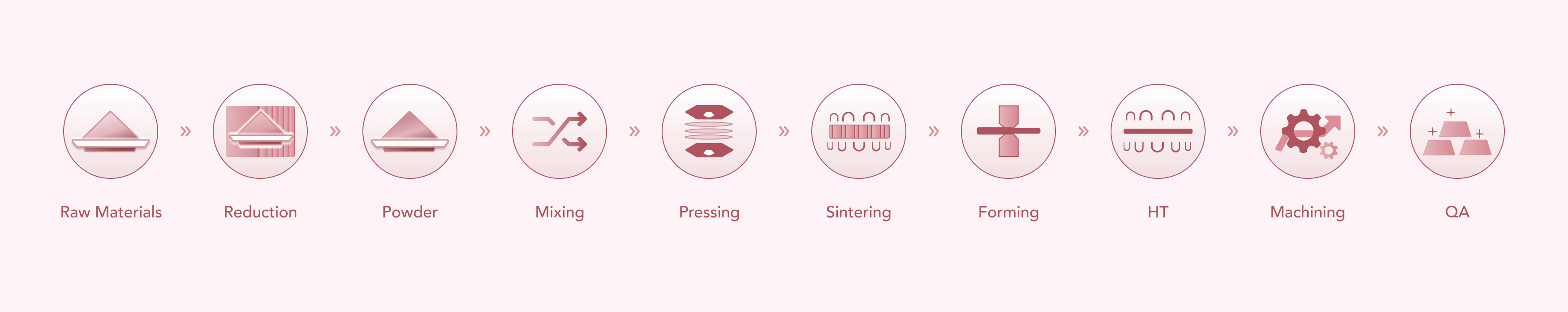
• Shaping: The pure niobium is then formed into the desired shape. Most often, the targets are made into discs or cylinders according to the sputtering system’s design. Consistent shape and size lead to more even film deposition.
• Bonding: In many cases, a backing material is attached to the niobium target. This extra layer helps manage the heat buildup during the sputtering process. It also extends the life of the target by reducing undue stress.
• Quality Testing: Before product release, every target goes through tests. Engineers check for uniformity, purity, and proper behavior under simulated sputtering conditions. This step ensures the targets will perform as expected when used in real applications.
Common Applications in Multiple Industries
Niobium sputtering targets find use in several critical areas:
• Electronics and Semiconductors: In tiny components like semiconductors, uniform thin films are very important. Niobium targets are used to deposit films that form parts of transistors, capacitors, or even solar cells. Electronics benefit from the consistent electrical conductivity and durability of the films.
• Solar Energy: Thin-film coatings on solar panels utilize the special properties of niobium. When these coatings reshape light or protect surfaces from harsh conditions, solar panels become more efficient and last longer.
• Aerospace and Automotive: Many engine components and heat shields require materials that resist extreme temperatures. Niobium’s high melting point ensures that the coatings stay intact even when exposed to very high heat.
These real-world cases make it clear how vital a role the niobium sputtering target plays in reliable modern technology.
Benefits of Using Niobium Sputtering Targets
There are many reasons why industries prefer niobium sputtering targets:
• Durability: Niobium’s natural resistance to corrosion ensures that its thin films maintain their properties over long periods. In harsh conditions, this durability is a major asset.
• Efficiency in Deposition: Because of its structure and purity, niobium targets release a consistent stream of atoms during sputtering. This results in even coatings that are important for device performance, especially in electronics.
• Heat Tolerance: The high melting point reduces the risk of the target deforming under high temperatures. This benefit is important in applications where heat is a persistent concern, such as in the aerospace field.
• Versatility in Applications: The same basic properties allow niobium to be used in many different industries. Whether applied to semiconductors, precision machinery, or protective layers, the reliability of niobium offers clear advantages.
Challenges and Practical Considerations
Despite its benefits, there are some practical issues to consider:
• Cost and Availability: High-quality niobium is not cheap. Extracting and refining the metal requires advanced methods, which can raise costs. In manufacturing, companies must balance these higher costs with the performance gains provided by niobium.
• Uniformity of Coating: While niobium has many positive traits, achieving a perfectly uniform film over large areas may be challenging. Special attention is needed during the sputtering process to maintain even distribution of the niobium atoms.
• Equipment Compatibility: Some older sputtering systems may require adjustments to work efficiently with a niobium target. Operators need practical knowledge and sometimes minor modifications to ensure successful deposition.
These challenges do not outweigh the benefits. Still, they remind us that every process has its practical aspects and that careful calibration and quality control are key to the best results.
Summary and Final Thoughts
Niobium sputtering targets have grown in importance as industries push for more resilient and efficient thin-film coatings. Their high melting point, resistance to chemical attack, and excellent conductivity make them a favorite for many applications. Although they come with their own set of challenges, the ability to work over a wide temperature range and in various environments makes niobium a material that continues to stand the test of time.
For those who need reliable sputtering targets for electronics, solar panels, aerospace parts, or other demanding uses, niobium provides a robust solution. In the end, understanding the properties and manufacturing processes helps engineers and technicians achieve a smoother, more consistent deposition process while ensuring the long-term durability of their components.
For trusted and quality materials, consider Stanford Advanced Materials (SAM) as your supplier. Their expertise in preparing high-quality niobium sputtering targets can provide a substantial benefit to your manufacturing and research endeavors.
Frequently Asked Questions
• Why choose niobium for sputtering targets?
Niobium offers a very high melting point, excellent resistance to corrosion by forming a protective oxide layer, and strong electrical conductivity. These features are critical for producing high-quality thin films.
• How is a niobium sputtering target made?
The process starts with purifying raw niobium. It is then shaped into a suitable form, often with an additional backing material to handle heat effectively. The final step involves careful quality tests to ensure performance in sputtering.
• What are typical applications for niobium sputtering targets?
They are mainly used to deposit thin films in electronics, solar panel coatings, and parts in the aerospace and automotive industries. Their properties make them ideal for environments with high heat and harsh chemicals.
• Are there any challenges with using niobium sputtering targets?
Yes, some issues include their higher cost due to extraction and purification, as well as ensuring an even coating during the sputtering process. With proper calibration and experience, these challenges can be managed effectively.


