Home
Product
Sputtering Target
By Chemical Elements
Evaporation Materials
By Evaporation Materials
By Chemical Elements
Bonding Service
Indium Target Bonding Service
OFHC Copper Backing Plates
Elastomeric Target Bonding Service
Planar Targets
Evaporation Sources
Thermal sources
E-Beam Source Used Crucibles
3D Printing Powder
Crystal Substrates
Thermal Spraying Coating
Application
Architectural, Automotive Glass & WEB Coating
Semiconductor Materials
Hardware & Decorative Coatings
Optics Coatings
Solar
Electronics
FAQ
About Us
NEWS
Blogs
Industry News
Most Popular
Contact Us
(949) 407-8904
Mon - Fri 08:00 - 17:00
1940 East Deere Avenue, Suite 100, Santa Ana, CA 92705, USA
Get A Quote
Home
Products
Sputtering Targets
By Material Types
By Chemical Elements
Evaporation Materials
By Material Types
By Chemical Elements
Precious Metals
Gold Sputtering Target
Silver Sputtering Target
Platinum Sputtering Target
Gold Evaporation Materials
Evaporation Source
Thermal Sources
Alumina Boat
E-Beam Source Used Crucibles
Graphite Crucible
Tungsten Crucible
Boron Nitride Crucible
Zirconia Crucible
Crystal Substrates
Calcium Carbonate Crystal
Barium Titanate Crystal
Rutile Titanium Dioxide Crystal
3D Printing Powders
Thermal Spraying Coating
Targets
By Target Shapes
Planar Sputtering Target
Rotary Sputter Target
Rare Earth Targets
Erbium Sputtering Target
Praseodymium Sputtering Target
Pure Metal Targets
Gold Sputtering Target
Iridium Sputtering Target
Aluminum Target
Alloy Targets
Ti/W Sputtering Target
Mo/Nb Alloy Rotary Target
Nb/Ti Sputtering Target
Oxide Targets
SiO2 Sputtering Target
Magnesium Oxide Target
Aluminum Oxide Sputtering Target
Nitride Targets
TiN Sputtering Target
AlN Sputtering Target
Boron Nitride Sputtering Target
Fluoride Targets
MgF2 Sputtering Target
LiF Sputtering Target
Carbide Targets
Silicon Carbide Sputtering Target
Fe3C Sputtering Target
Pellets
Pure Metal Pellets
Gold Evaporation Materials
Alloy Pellets
Oxide Pellets
Nitride Pellets
Niobium Nitride Evaporation Materials
Fluoride Pellets
Magnesium Fluoride Evaporation Materials
Carbide Pellets
Iron Carbide Evaporation Materials
Silicide Pellets
Sulfide Pellets
Boride Pellets
Selenide Pellets
Services
Target Bonding
Indium Bonding
Copper Backing Plates
Elastomeric Bonding Service
Target Recycling
Applications
Solar
CIGS Sputtering Target
Semiconductors
Electronics
Lithium Niobate Sputtering Target
Optics Coatings
Hardware & Decorative Coatings
Automotive Glass & WEB Coating
About
Blogs
Cornerstone Articles
What is Physical Vapor Deposition (PVD)?
What is Chemical Vapor Deposition (CVD)? The Ultimate Guide
Glossary
Terms & Conditions
MSDS Listings
Privacy Policy
Friend Links
FAQ
Inquiry
Tag
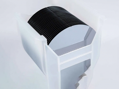
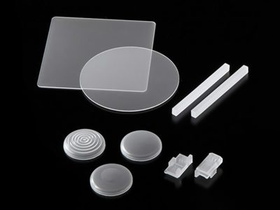
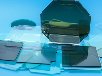
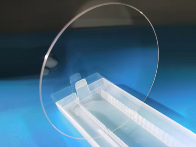
Substrate/Wafer
January 22, 2025
Julissa Green
Applications
,
Blog
,
Guides & How-to
Silicon on Insulator (SOI) Technology and Its Application Prospects
I. Introduction Silicon-on-insulator (SOI) technology represents a pivotal advancement in semiconductor manufacturing, offering enhanced performance...
January 2, 2025
Julissa Green
Blog
,
Comparison
,
Guides & How-to
Comprehensive Guide to Dielectric Substrates: Key Materials and Applications
Introduction Dielectric substrates are indispensable materials in modern electronic devices. They play a crucial role...
August 21, 2024
Julissa Green
Blog
The Benefits and Applications of SiC Crystal Substrates
Silicon carbide (SiC) crystal substrates are advanced semiconductor materials with unique properties. These substrates have...
June 25, 2024
Julissa Green
Blog
An Overview of Transparent Conductive Oxides (TCOs)
1. Introduction Transparent Conductive Oxides (TCOs) are a unique class of materials that combine two...
May 7, 2024
Julissa Green
Blog
CVD Diamond Wafers Revolutionizing Industries
Introduction Synthetic diamonds, particularly those produced by Chemical Vapor Deposition (CVD), represent a significant technological...
April 24, 2024
Julissa Green
Applications
,
Blog
Magnesium Oxide Target in Thin-Film Transistors Production
Thin-film transistors (TFTs) are fundamental components in a myriad of electronic devices that shape our...
March 27, 2024
Julissa Green
Blog
Yttrium Iron Garnet Explained: From Crystal Structure to Technological Marvels
Introduction Yttrium Iron Garnet (YIG), with its enigmatic presence in the domain of material science,...
July 19, 2023
Julissa Green
Blog
A Comprehensive Guide to Gallium Arsenide (GaAs) Wafers
Introduction Gallium Arsenide (GaAs) wafers have revolutionized the world of semiconductor technology with their...
July 11, 2023
Julissa Green
Blog
Driving Innovation with Gallium Arsenide (GaAs) Wafers: Advancements in Semiconductor Technology
Introduction Semiconductor technology has been at the forefront of driving innovation in various industries, ranging...
1
2
Product categories
Sputtering Target
Alloy Targets
By Chemical Elements
Ceramic Targets
Other Compound Targets
Pure Metal Targets
Advanced Materials
3D Printing Powder
Crystals & Substrates
Specialty Wires & Foils
Thermal Spraying Coating
Bonding Service
Elastomeric Target Bonding Service
Indium Target Bonding Service
OFHC Copper Backing Plates
Evaporation Materials
Alloy Evaporation Materials
By Chemical Elements
By Evaporation Materials
Ceramic Evaporation Materials
Metal
Evaporation Sources
E-Beam Source Used Crucibles
Thermal sources
Featured Products
ST0033 Niobium Sputtering Target, Nb
ST6843 Silicon (Si) Rotary Sputtering Target
ST11173 Sodium Phosphate (Na3PO4) Sputtering Target
ST11221 Zinc Sulfide (ZnS) Planar Sputtering Target
ST11220 Zinc (Zn) Rotary Sputtering Target