A Comprehensive Guide to Gallium Arsenide (GaAs) Wafers
See our Gallium Arsenide Wafer Product
Introduction
Gallium Arsenide (GaAs) wafers have revolutionized the world of semiconductor technology with their exceptional performance and unique properties. In this comprehensive guide, we will explore the power of GaAs wafers and delve into their applications, fabrication process, and key benefits.
1. Understanding GaAs Wafers:
GaAs wafers are composed of gallium (Ga) and arsenic (As) atoms. This semiconductor material shows remarkable properties such as high electron mobility, high breakdown voltage, and excellent thermal stability, which make them highly suitable for applications requiring high-frequency operation, low noise, and high power efficiency.
2. Fabrication Process:
The fabrication process of GaAs wafers involves several steps to ensure high-quality and precise performance.
- The process typically includes crystal growth through techniques like molecular beam epitaxy (MBE) or metal-organic chemical vapor deposition (MOCVD).
- After crystal growth, the wafer is subjected to various processes, including polishing, cleaning, and etching, to obtain a smooth and defect-free surface.
- Advanced lithography and etching techniques are used to pattern the wafer for specific device structures.
3. Key Benefits of GaAs Wafers:
Quality GaAs wafers stand out for the following good points.
- High Electron Mobility: GaAs wafers exhibit higher electron mobility compared to silicon, enabling faster device operation and higher frequency capabilities. This property is crucial in applications that require high-speed signal processing, such as wireless communication systems and high-speed data transfer.
- Low Resistivity: The resistivity of GaAs wafers is lower than silicon, reducing the resistance encountered by charge carriers, which is essential for high-speed devices as it minimizes power losses and signal degradation. The lower resistivity also allows for efficient charge transport and enables devices to operate at higher speeds with improved power efficiency.
- Wide Bandgap: The wider bandgap enables the production of high-performance optoelectronic devices. These devices include light-emitting diodes (LEDs), laser diodes, and photodetectors used in applications such as optical communications, display technologies, and solid-state lighting. Also, the wide bandgap brings about the emission and detection of light across a broader range of wavelengths, resulting in enhanced device performance and efficiency.
- Low Noise Performance: Such wafers have inherently low noise characteristics, making them suitable for applications that demand high signal-to-noise ratios. This is significant in fields like telecommunications and radio frequency (RF) systems, where signal integrity and sensitivity are essential.
- Thermal Stability: They possess excellent thermal stability, allowing them to withstand high operating temperatures without significant degradation in performance. Therefore, these wafers are applied to fields where high-power dissipation and thermal management are critical.
Related reading: Gallium Arsenide Wafer VS. Silicon Wafer
4. Applications of GaAs Wafers:
As an alternative to traditional silicon wafers, GaAs wafers offer a range of advantages that make them highly valuable in various applications.
- Telecommunications: GaAs wafers are widely employed in the telecommunications industry for the fabrication of devices such as high-speed transistors, laser diodes, and photodetectors. Their ability to operate at high frequencies makes them ideal for applications in wireless communication, satellite communication, and fiber-optic networks.
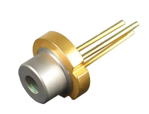
- Optoelectronics: GaAs-based optoelectronic devices, including light-emitting diodes (LEDs) and laser diodes, offer superior performance in terms of efficiency and wavelength range. GaAs wafers are also crucial in the production of these devices, enabling advancements in optical communications, solid-state lighting, and display technologies.
- High-Frequency Electronics: GaAs wafers are used in high-frequency electronic circuits, such as power and low-noise amplifiers, due to their high electron mobility and low noise characteristics. These properties are particularly beneficial in applications like radar systems, satellite communication, and wireless networks.
Conclusion
In short, GaAs wafers have emerged as a powerful alternative to silicon wafers in telecommunications, optoelectronics, high-frequency electronics, and various industries because of their high electron mobility, wide bandgap, low noise performance, and thermal stability. As technology advances, these wafers will play a crucial role in enabling innovative solutions and driving progress in a wide range of applications, ultimately shaping the future of semiconductor technology.
Stanford Advanced Materials (SAM) has rich experience in manufacturing and selling quality gallium arsenide wafers. A variety of wafers and sputtering devices are available on our website. Please visit our homepage for more information.
Inquiry SAM's GaAs Wafer Product


