Driving Innovation with Gallium Arsenide (GaAs) Wafers: Advancements in Semiconductor Technology
Introduction
Semiconductor technology has been at the forefront of driving innovation in various industries, ranging from telecommunications and consumer electronics to renewable energy and aerospace. Within the realm of semiconductors, Gallium Arsenide (GaAs) wafers have emerged as a powerful tool, fueling advancements in semiconductor devices and enabling the development of cutting-edge technologies. In this article, we will explore how GaAs wafers are driving innovation and revolutionizing semiconductor technology.
Understanding GaAs Wafers
GaAs wafers are compound semiconductor materials containing gallium (Ga) and arsenic (As) atoms. Unlike traditional silicon wafers, GaAs wafers offer unique electronic properties that make them highly desirable in semiconductor applications. GaAs is a direct bandgap material, meaning it can efficiently emit and absorb light, making it ideal for optoelectronic devices. Additionally, GaAs has high electron mobility and excellent carrier velocity, allowing for high-speed electronic applications.
Related reading: Gallium Arsenide Wafer VS. Silicon Wafer
GaAs Wafers: Advancement in Semiconductor Devices
With these promising features, GaAs wafers are applied to a variety of industries, especially the semiconductor field.
–High-Frequency Applications
One of the significant semiconductor applications of GaAs wafers is high-frequency devices. Such equipment is commonly seen in the field of telecommunications, satellite communication systems, and radar technology, where high-frequency operation is essential.
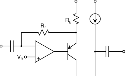
Besides, GaAs-based devices, including high-electron-mobility transistors (HEMTs) and heterojunction bipolar transistors (HBTs), enable the development of high-frequency amplifiers and signal processing circuits that offer superior performance and faster data rates.
–Optoelectronics and Photonics
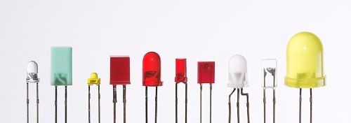
GaAs wafers have also revolutionized the field of optoelectronics by enabling the development of advanced devices such as light-emitting diodes (LEDs), laser diodes, and photodetectors.
GaAs-based LEDs offer higher efficiency, brighter output, and better color accuracy compared to traditional light sources. Laser diodes based on GaAs wafers are widely used in applications such as fiber-optic communications, optical storage systems, and medical equipment. GaAs photodetectors, on the other hand, provide excellent sensitivity and response time, facilitating high-speed optical communication and sensing applications.
–Power Electronics
GaAs wafers have made significant contributions to power electronics, particularly in applications where high power density and efficiency are required.
GaAs-based power devices, such as Schottky diodes and high-power transistors, exhibit low on-resistance, fast switching speeds, and low power losses. These characteristics make GaAs-based power devices well-suited for high-frequency power amplifiers, voltage regulators, and energy conversion systems, contributing to increased energy efficiency and compact designs.
GaAs Wafers: Emerging Technologies
GaAs wafers have become popular materials for the following advanced technologies thanks to their desirable features and great potential.
–5G Wireless Communications
The rollout of 5G wireless networks demands higher data rates, lower latency, and increased network capacity. Therefore, GaAs wafers play a crucial role in enabling the development of high-frequency millimeter-wave transceivers and power amplifiers that are essential for 5G communication systems. The high-frequency capabilities and power efficiency of GaAs-based devices are instrumental in delivering the performance requirements of 5G networks.
–Quantum Computing
Quantum computing is a rapidly evolving field that aims to revolutionize computation by leveraging the principles of quantum mechanics. GaAs wafers have shown promise in the development of qubits, the building blocks of quantum computers. GaAs-based quantum dots have demonstrated long coherence times and robustness against noise, making them a potential candidate for quantum information processing.
GaAs Wafers: Future Prospects
As semiconductor technology continues to advance, GaAs wafers are expected to play an increasingly significant role. Ongoing research and development efforts focus on enhancing the performance of GaAs-based devices, improving manufacturing processes, and exploring new device architectures. Furthermore, the integration of GaAs wafers with other semiconductor materials, such as silicon, enables the creation of hybrid devices that combine the strengths of both materials.
Conclusion
In a word, Gallium Arsenide (GaAs) wafers are driving innovation in semiconductor technology. Their unique electronic properties and versatility have opened doors to advancements in high-frequency applications, optoelectronics, power electronics, and emerging technologies. As we continue to harness the potential of GaAs wafers, we can expect to see further breakthroughs in various industries, shaping the future of semiconductor technology.
Stanford Advanced Materials (SAM) has rich experience in the manufacturing and sale of quality gallium arsenide wafers. Customization is also welcome. For more information, please visit our homepage.
Reference:
[1] Baumbaugh, A. (1998). Charge integrator and encoder ASIC for readout of the CMS hadron calorimeter photodetectors.
[2] Light-emitting diode. (2023, June 16). In Wikipedia. https://en.wikipedia.org/wiki/Light-emitting_diode


