| Catalog No. | GA2171 |
|---|---|
| Material | GaAs |
| Thickness | 350 um ~ 625 um |
| Conductive Type | P – type / N – type / Semi-insulating |
| Diameter | Ø 2″ / Ø 3″ / Ø 4″ |
| Polytype | 4H / 6H |
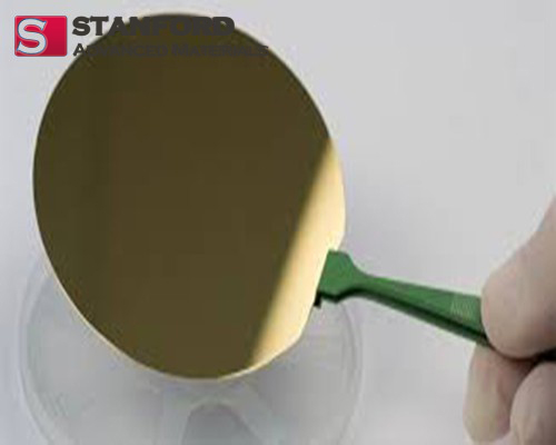
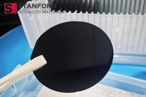
Stanford Advanced Materials (SAM) offer single crystal GaAs gallium arsenide wafer produced by two main growth techniques LEC and VGF method, allowing us to provide customers the widest choice of GaAs material with high uniformity of electrical properties and excellent surface quality.
Gallium Arsenide (GaAs) wafers are a crucial material in high-performance electronics and optoelectronics. With their unique properties, such as high electron mobility and excellent thermal stability, GaAs wafers are widely used in applications like LEDs, laser diodes, and solar cells. Our GaAs wafers are available in both semi-insulating and conducting forms, making them ideal for a variety of applications across different industries.
Key Features of Our GaAs Wafers
|
Growth |
LEC / VGF |
|
Diameter |
Ø 2″ / Ø 3″ / Ø 4″ |
|
Thickness |
350 um ~ 625 um |
|
Orientation |
<100> / <111> / <110> or others |
|
Conductivity |
P – type / N – type / Semi-insulating |
|
Dopant |
Zn / Si / undoped |
|
Surface |
One side polished or two sides polished |
|
Concentration |
1E17 ~ 5E19 cm-3 |
|
TTV |
<= 10 um |
|
Bow / Warp |
<= 20 um |
|
Grade |
Epi polished grade / mechanical grade |
We offer a range of GaAs wafers, including the following types:
Each wafer type is available in different grades, such as epitaxial-ready (epi-ready) and polished surfaces, ensuring high performance for your specific needs.
GaAs wafers are widely used in many high-tech applications:
Our Gallium Arsenide wafers are designed to meet the highest standards of quality and performance. Whether you need GaAs wafers for research, prototyping, or mass production, we offer a reliable supply of top-quality wafers to suit your needs.
Send A Inquiry
Related Article:
Gallium Arsenide Wafer VS. Silicon Wafer
What Are the Benefits of Gallium Phosphide Wafers?
Gallium Arsenide Wafer Used for Electronic Devices Manufacturing
What Are P-type & N-type Silicon Semiconductors
Submit your review | |
Great quality gallium arsenide wafer! Perfect for my research project. The wafers arrived on time and were well-packaged. Highly recommend for anyone needing reliable materials for optoelectronics!
Excellent product! Used these GaAs wafers for our laser diode prototypes, and they performed flawlessly. Will definitely order again for future projects. The customer service was also top-notch!