Gallium Arsenide Wafer Used for Electronic Devices Manufacturing
Introduction
Gallium Arsenide (GaAs) wafers have a variety of applications in the field of electronics, particularly in the production of high-performance electronic devices. In this article, we will explore some common applications of GaAs wafers for electronic device manufacturing and provide a better understanding of their properties and advantages.
Properties of Gallium Arsenide Wafer
Gallium arsenide is a group III-V semiconductor material with unique electronic, optical, and other properties.
- Electronic: Gallium arsenide wafers are characterized by impressive electron mobility that is about five times silicon. Such mobility is related to their structure. The bonds between arsenic and gallium atoms are prone to break with sufficient energy. Consequently, electrons come out and move freely.
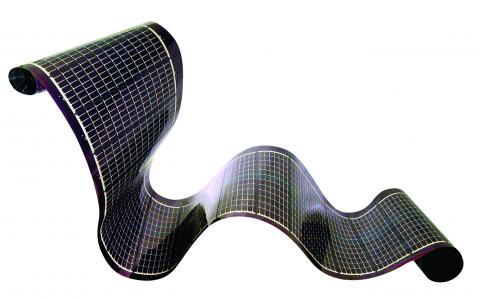
- Optical: GaAs wafers stand out for their direct bandgap. Namely, electrons could move through quickly, and photons can pass through with ease. This makes them popular materials for laser diodes, solar cells, and other optoelectronics.
- Others: GaAs also has outstanding low reverse saturation currents, high breakdown voltages, great flexibility, wide operating temperature range, and heat and moisture resistance.
Thanks to these characteristics, gallium arsenide wafers are applied to manufacture electronics, optical devices, and other high frequency-tools.
Related reading: Gallium Arsenide Wafer VS. Silicon Wafer
Uses of Gallium Arsenide Wafer in Electronic Devices Manufacturing
High-frequency Devices
GaAs wafers are used in the production of high-frequency devices such as microwave transistors, amplifiers, and oscillators. This is because they have higher electron mobility than other semiconductor materials, allowing for faster and more efficient movement of electrons through the material.
Power Electronic Devices
GaAs wafers are employed to prepare power electronic devices such as high-power amplifiers and transistors because they have a higher thermal conductivity than Si, which allows for better heat dissipation and makes GaAs-based devices less prone to overheating.
High-speed Communication Devices
Gallium arsenide wafers are choice semiconductors for high-speed communication devices such as optical modulators and switches. The reason is that GaAs-based devices can operate at much higher frequencies than Si-based devices, making them ideal for high-speed data transfer and communication. The conductivity of GaAs wafers ensures the efficient flow of electrical current through the device, and GaAs entered the markets of wireless local area networks (WLAN), global positioning systems (GPS), etc.
Photovoltaic Cells
GaAs has a high absorption coefficient for sunlight, which allows for the efficient conversion of solar energy into electrical energy. Therefore, these wafers are prepared to manufacture photovoltaic cells for solar energy conversion. You can find GaAs-based solar on the Opportunity and Spirit rovers. Additionally, GaAs possesses resistance to radiation damage, which leads to its use in optical windows, space electronics, and other optical apparatus.
Integrated Circuits and Microprocessors
Since GaAs-based devices can be made smaller and more densely packed than Si-based devices, allowing for more complex and powerful electronics to be produced in a smaller space, these wafers are widely utilized to make integrated circuits and microprocessors. High-performance chips can be produced on a single slice of GaAs.
Sensors and Detectors
GaAs wafers are applied to produce sensors and detectors for various applications such as medical, environmental, and scientific purposes. This is because GaAs has a high sensitivity to electromagnetic radiation, making it useful for detecting and measuring electromagnetic waves such as light and radio waves.
Conclusion
In a word, gallium arsenide wafers have a wide range of applications in the manufacturing of electronic devices, including high-frequency devices, power electronics, high-speed communication devices, photovoltaic cells, integrated circuits, and sensors and detectors. The desirable properties of GaAs wafers, including high electron mobility, direct bandgap, high thermal conductivity, a high absorption coefficient for sunlight, and a wide operating temperature range, make them ideal for a wide range of applications where performance, efficiency, and accuracy are essential. As technology continues to advance, it is likely that we will see even more innovative applications of GaAs wafers in the future.
Stanford Advanced Material (SAM) provides quality gallium arsenide wafers for a variety of applications. Hope that you can select the perfect wafers for your projects. For more information, please check our homepage.


