What Are the Benefits of Gallium Phosphide Wafers?
See our Gallium Arsenide Wafer Product
Introduction
Gallium phosphide (GaP) is a compound semiconductor material that has gained increasing attention in the semiconductor industry. GaP wafers offer several advantages over traditional silicon wafers, including high efficiency, high-speed operation, and high power handling capabilities. In this article, we will talk about the benefits of using gallium phosphide wafers in electronic and optical devices. Hope that you can have a better understanding of the properties and uses of gallium phosphide wafers.
What Are Gallium Phosphide Wafers?
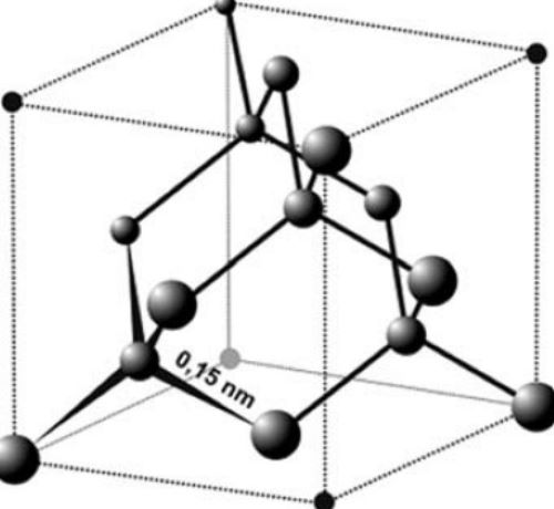
Gallium phosphide (GaP) wafer is a promising semiconductor component. Wafers made from gallium phosphide have the following properties. These orange wafers are odorless and insoluble in water. As for optical features, they have an indirect band gap of 2.24 eV at room temperature. Additionally, GaP wafers share a similar crystal structure as silicon.
With all these desirable features, gallium phosphide wafers find applications in optical devices and electronic equipment, such as light-emitting diodes (LEDs) and solar cells.
Benefits of Gallium Phosphide Wafers
–High Efficiency
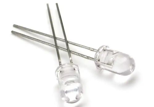
Firstly, GaP wafers offer high efficiency. GaP has a direct bandgap, which means that it can efficiently emit light. This property makes GaP wafers ideal for use in optoelectronic devices, such as light-emitting diodes (LEDs), solar cells, and laser diodes. GaP has higher energy conversion efficiency than other semiconductor materials, such as silicon, making it perfect for use in high-performance solar cells. GaP solar cells have achieved efficiency levels of up to 20%, making them competitive with traditional silicon solar cells.
Let’s have a further discussion about the highly efficient optical applications of GaP wafers. Gallium phosphide substrates are widely used to produce red, green, yellow, and orange visible LEDs because they are transparent to those wavelengths. These low-price LEDs come with numerous optical properties. You can also dope zinc oxide and nitrogen for longer wavelength emission.
–High Electron Mobility
Secondly, gallium phosphide wafers provide high-speed operation because of their special structure. The crystal structure of GaP is similar to silicon, yet its gallium and phosphorus atoms are on adjacent sites. A single silicon atom has 14 electrons, while 4 electrons locate on the outermost circle. These electrons do not shift around, so there would be no electric current. Phosphorus has one more electron than silicon. If you substitute an atom of phosphorus, you will have one extra electron, which can move freely and generate current flow consequently.
In this way, electrons move more quickly through the material, and GaP has higher electron mobility than silicon. This property makes GaP wafers the choice materials for high-frequency electronic devices, such as high-frequency transistors and amplifiers. GaP-based devices have demonstrated high-speed operation, with transistor cutoff frequencies exceeding 500 GHz as well.
–New Advanced Devices
Gallium phosphide wafers stand out for their potential for new device applications. The unique properties of GaP make it an ideal material for developing new electronic devices. GaP-based devices, such as GaP-based LEDs and solar cells, have already been demonstrated, and there is potential for new devices, such as high-power GaP-based lasers and GaP-based sensors.
Let’s take a look at the specific case of gallium phosphide optical metasurfaces. Gallium phosphide is a great semiconductor material for developing such advanced devices. It has an indirect bandgap of 2.24 eV. GaP is also transparent in the visible spectrum (wavelength λ>0.54 µm), which is much higher than titanium oxide (n=2.4–2.7) and hafnium oxide (n=1.9). [2]
–Other Advantages
GaP wafers offer high power handling capabilities. GaP has a high breakdown voltage, which means that it can withstand high voltages without breaking down. This characteristic makes GaP wafers popular for use in high-power electronic devices, including power amplifiers and switches. GaP devices have demonstrated high-power handling capabilities, with power densities exceeding 10 W/mm.
Another benefit of GaP wafers is their compatibility with existing manufacturing processes. GaP can be grown using Metal-Organic Chemical Vapor Deposition (MOCVD) and Molecular Beam Epitaxy (MBE) techniques, which are already extensively used in the semiconductor industry. This means that GaP wafers can be easily integrated into existing manufacturing processes, making them an attractive option for semiconductor manufacturers.
Conclusion
In a word, gallium phosphide wafers are known for their high efficiency, high-speed operation, high power handling capabilities, compatibility with existing manufacturing processes, and potential for new device applications. They have countless advantages over traditional silicon wafers.
Thus, GaP wafers are an attractive option for semiconductor manufacturers looking to develop high-performance electronic devices. Stanford Advanced Materials (SAM) is a supplier of gallium phosphide wafers of various diameters and thicknesses. Send us an inquiry if you are interested.
Reference:
[1] Daillant, J., & Gibaud, A. (2008). X-Ray and Neutron Reflectivity: Principles and Applications [Photograph]. https://www.researchgate.net/publication/253299488_X-Ray_and_Neutron_Reflectivity_Principles_and_Applications
[2] Melli, M., West, M., Hickman, S. et al. (2020). Gallium phosphide optical metasurfaces for visible light applications. Nature. https://doi.org/10.1038/s41598-020-77753-0
Inquiry SAM's GaAs Wafer Product


