Home
Product
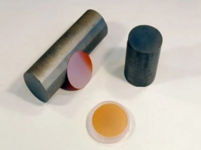
Sputtering Target
By Chemical Elements
Evaporation Materials
By Evaporation Materials
By Chemical Elements
Bonding Service
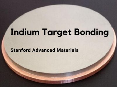
Indium Target Bonding Service
OFHC Copper Backing Plates
Elastomeric Target Bonding Service
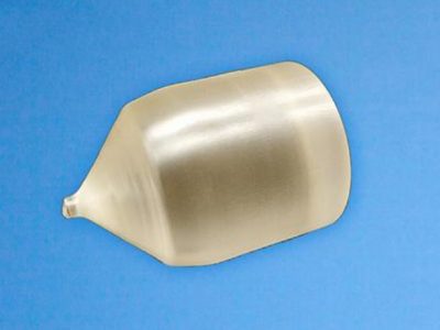
Planar Targets
Evaporation Sources
Thermal sources
E-Beam Source Used Crucibles
3D Printing Powder
Crystal Substrates
Thermal Spraying Coating
Application
Architectural, Automotive Glass & WEB Coating
Semiconductor Materials
Hardware & Decorative Coatings
Optics Coatings
Solar
Electronics
FAQ
About Us
NEWS
Blogs
Industry News
Most Popular
Contact Us
(949) 407-8904
Mon - Fri 08:00 - 17:00
1940 East Deere Avenue, Suite 100, Santa Ana, CA 92705, USA
Get A Quote
Home
Products
Sputtering Targets
By Material Types
By Chemical Elements
Evaporation Materials
By Material Types
By Chemical Elements
Precious Metals
Gold Sputtering Target
Silver Sputtering Target
Platinum Sputtering Target
Gold Evaporation Materials
Evaporation Source
Thermal Sources
Alumina Boat
E-Beam Source Used Crucibles
Graphite Crucible
Tungsten Crucible
Boron Nitride Crucible
Zirconia Crucible
Crystal Substrates
Calcium Carbonate Crystal
Barium Titanate Crystal
Rutile Titanium Dioxide Crystal
3D Printing Powders
Thermal Spraying Coating
Targets
By Target Shapes
Planar Sputtering Target
Rotary Sputter Target
Rare Earth Targets
Erbium Sputtering Target
Praseodymium Sputtering Target
Pure Metal Targets
Gold Sputtering Target
Iridium Sputtering Target
Aluminum Target
Alloy Targets
Ti/W Sputtering Target
Mo/Nb Alloy Rotary Target
Nb/Ti Sputtering Target
Oxide Targets
SiO2 Sputtering Target
Magnesium Oxide Target
Aluminum Oxide Sputtering Target
Nitride Targets
TiN Sputtering Target
AlN Sputtering Target
Boron Nitride Sputtering Target
Fluoride Targets
MgF2 Sputtering Target
LiF Sputtering Target
Carbide Targets
Silicon Carbide Sputtering Target
Fe3C Sputtering Target
Pellets
Pure Metal Pellets
Gold Evaporation Materials
Alloy Pellets
Oxide Pellets
Nitride Pellets
Niobium Nitride Evaporation Materials
Fluoride Pellets
Magnesium Fluoride Evaporation Materials
Carbide Pellets
Iron Carbide Evaporation Materials
Silicide Pellets
Sulfide Pellets
Boride Pellets
Selenide Pellets
Services
Target Bonding
Indium Bonding
Copper Backing Plates
Elastomeric Bonding Service
Target Recycling
Applications
Solar
CIGS Sputtering Target
Semiconductors
Electronics
Lithium Niobate Sputtering Target
Optics Coatings
Hardware & Decorative Coatings
Automotive Glass & WEB Coating
About
Blogs
Cornerstone Articles
What is Physical Vapor Deposition (PVD)?
What is Chemical Vapor Deposition (CVD)? The Ultimate Guide
Glossary
Terms & Conditions
MSDS Listings
Privacy Policy
Friend Links
FAQ
Inquiry
Category
Blog
May 11, 2023
Julissa Green
Blog
Gallium Arsenide Wafer Used for Electronic Devices Manufacturing
Introduction Gallium Arsenide (GaAs) wafers have a variety of applications in the field of electronics,...
May 3, 2023
Julissa Green
Blog
Practical Methods to Increase Deposition Rate
Introduction The deposition rate is an important factor in the field of thin film deposition,...
April 6, 2023
Julissa Green
Blog
What Are the Benefits of Gallium Phosphide Wafers?
Introduction Gallium phosphide (GaP) is a compound semiconductor material that has gained increasing attention...
March 21, 2023
Julissa Green
Blog
Gadolinium Gallium Garnet: Properties, Manufacturing & Applications
Introduction Garnets (A3B2(SiO4)3) are a group of minerals commonly used as substrates, abrasives, and gemstones....
March 14, 2023
Julissa Green
Blog
What Is Indium Bonding for Sputtering Target?
Introduction to Indium Bonding Target bonding is a significant process that joins sputtering targets and...
March 1, 2023
Julissa Green
Blog
Gallium Arsenide Wafer VS. Silicon Wafer
Introduction With the development of electronic devices, people pay more and more attention to wafers,...
February 21, 2023
Julissa Green
Blog
An Overview of Terbium Sputtering Targets
Introduction Terbium sputtering targets are made from terbium metal. They are used widely in a...
February 13, 2023
Julissa Green
Blog
Do Impurities Always Have A Negative Effect on Sputtering?
Introduction Purity is one of the prime performance requirements of target selection, which has been...
February 6, 2023
Julissa Green
Blog
,
Industrial News
What Are the Most Important Characteristics of Sputtering Target Selection
1. Introduction to Sputtering Target Selection The target quality is rather significant for the coating...
1
…
14
15
16
17
18
…
33
Product categories
Sputtering Target
Alloy Targets
By Chemical Elements
Ceramic Targets
Other Compound Targets
Pure Metal Targets
Advanced Materials
3D Printing Powder
Crystals & Substrates
Specialty Wires & Foils
Thermal Spraying Coating
Bonding Service
Elastomeric Target Bonding Service
Indium Target Bonding Service
OFHC Copper Backing Plates
Evaporation Materials
Alloy Evaporation Materials
By Chemical Elements
By Evaporation Materials
Ceramic Evaporation Materials
Metal
Evaporation Sources
E-Beam Source Used Crucibles
Thermal sources
Featured Products
ST0033 Niobium Sputtering Target, Nb
ST6843 Silicon (Si) Rotary Sputtering Target
ST11173 Sodium Phosphate (Na3PO4) Sputtering Target
ST11221 Zinc Sulfide (ZnS) Planar Sputtering Target
ST11220 Zinc (Zn) Rotary Sputtering Target