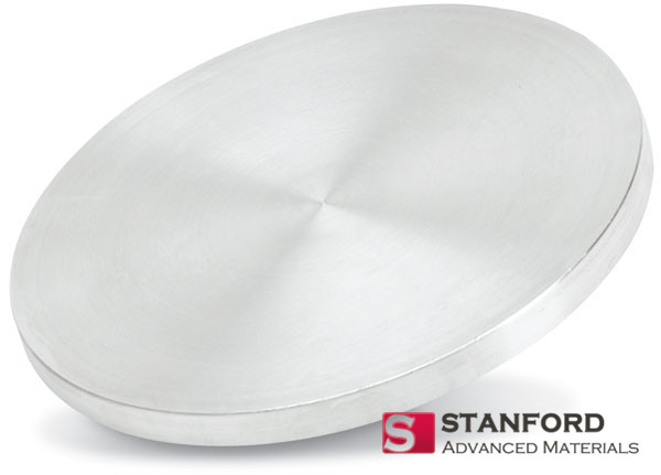
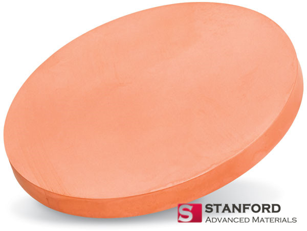
| Material | AlGaSb |
| Purity | 99.9% |
| Shape | Planar Disc |
The Aluminum Gallium Antimonide (AlGaSb) Target is a versatile ternary III-V compound that offers a blend of superior electronic, structural, and thermal properties, making it ideal for sophisticated thin-film applications. Typically crystallizing in the zinc blende structure, AlGaSb exhibits excellent lattice compatibility with other III-V semiconductors such as GaSb and InAs, facilitating seamless integration into heterostructure devices. By varying the ratio of Aluminum to Gallium, the bandgap of AlGaSb can be precisely engineered within the range of 0.5 to 1.6 eV. This tunability allows for tailored electrical and optical characteristics to meet specific device requirements. AlGaSb boasts high carrier mobility and low effective mass, which are crucial for developing high-speed and energy-efficient electronic devices. Additionally, it offers robust thermal stability and chemical inertness under controlled conditions. When processed as a sputtering target, AlGaSb achieves high density and uniform grain distribution, ensuring consistent and high-quality thin film deposition. Its semiconducting resistivity can be adjusted based on composition and doping, providing flexibility for various applications.
Material: Aluminum Gallium Antimonide (AlGaSb)
Purity: 99.9%
Shape: Planar Disc
Sputtering Methods: RF, DC, Molecular Beam Epitaxy (MBE)
Bonding Types: Indium, Elastomer
Note: Specifications are based on theoretical data. For customized requirements and detailed inquiries, please contact us.
Customized sizes are available to accommodate specific project requirements.
The Aluminum Gallium Antimonide (AlGaSb) Target is predominantly utilized in the manufacturing of advanced optoelectronic and high-speed electronic devices. Its adjustable bandgap and excellent lattice matching make it perfect for:
Our AlGaSb Targets are meticulously packaged to ensure their integrity during transportation and storage. Depending on the size, smaller targets are securely placed in polypropylene (PP) boxes, while larger targets are shipped in custom wooden crates. We prioritize customized packaging solutions and utilize appropriate cushioning materials to guarantee maximum protection.
Packaging Options:
Q1: What deposition techniques are compatible with AlGaSb targets?
A1: AlGaSb targets are typically utilized in sputtering and molecular beam epitaxy (MBE) systems. Ensuring proper chamber conditions and substrate matching is crucial for achieving high-quality thin films.
Q2: How should AlGaSb targets be stored?
A2: AlGaSb targets should be stored in a clean, dry, and vacuum-sealed environment to prevent surface oxidation and contamination. Using inert gas packaging is recommended during transportation.
Q3: Can SAM provide custom sizes and shapes?
A3: Yes, Stanford Advanced Materials (SAM) offers custom dimensions, bonding services, and configurations (planar, rotary) to suit a wide range of deposition systems.
| Property | AlGaSb Target (Aluminum Gallium Antimonide) | GaSb Target (Gallium Antimonide) | InSb Target (Indium Antimonide) | AlAs Target (Aluminum Arsenide) |
|---|---|---|---|---|
| Purity | ≥99.95% (MBE/PVD synthesis) | ≥99.9% (Czochralski growth) | ≥99.8% (zone refining) | ≥99.95% (epitaxial grade) |
| Thermal Stability (°C) | ≤600 | ≤550 | ≤400 | ≤900 |
| Bandgap (eV) | 0.7-1.6 | 0.72 | 0.17 | 2.16 |
| Thermal Conductivity (W/m·K) | 20-30 | 32 | 18 | 90 |
| Mechanical Strength (MPa) | 300-350 | 250-300 | 150-200 | 400-450 |
| Sputtering Rate (nm/min) | 100-150 (RF, 400W) | 80-120 (DC, 300W) | 50-80 | 200-250 |
Physical Properties:
Chemical Properties:
Aluminum is a lightweight, silvery-white metal known for its exceptional corrosion resistance, high thermal and electrical conductivity, and low density. It forms a natural oxide layer that protects it from further oxidation, making it ideal for coating other metals to prevent rusting. Aluminum is also highly reflective and easily alloyed with other metals, enhancing its versatility in various industrial applications.
Industrial Applications:
Physical Properties:
Chemical Properties:
Gallium is a soft, silvery metal with a melting point slightly above room temperature, allowing it to melt in the hand. It is widely used in semiconductors, optoelectronics, and various compound materials due to its excellent electronic properties. Gallium forms stable compounds with elements such as arsenic (GaAs), nitrogen (GaN), and antimony (GaSb), which are crucial in high-speed and high-frequency electronic devices. Its ability to alloy with other metals and its significant role in photovoltaic and LED technologies make gallium a valuable material in modern electronics.
Industrial Applications:
Physical Properties:
Chemical Properties:
Antimony is a lustrous, brittle metalloid extensively used in semiconductor materials, flame retardants, and various alloys. It enhances the hardness and strength of metals and forms important semiconducting compounds such as antimonides. In thin film technology, antimony compounds like GaSb and InSb are prized for their excellent thermoelectric and infrared detection properties. Antimony’s unique ability to modify the electrical conductivity of materials makes it indispensable in advanced electronics and energy applications.
Industrial Applications: