Everything You Need to Know About Tungsten Sputter Targets
Introduction
Sputter deposition, a pivotal technique in thin-film coatings, utilizes physical vapor deposition (PVD) to create material films on various substrates. Among the materials used for sputter targets, tungsten stands out due to its significant properties and applications in various high-tech industries. This article delves into the world of tungsten sputter targets, exploring their characteristics, manufacturing processes, and broad utility in applications ranging from electronics to automotive components. By understanding the nuances of tungsten as a sputter target, industries can leverage its properties to enhance product performance and durability, marking its critical role in advancing modern technology.
Understanding Tungsten Sputter Targets
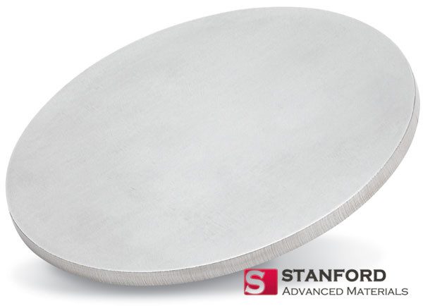
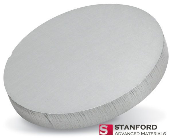
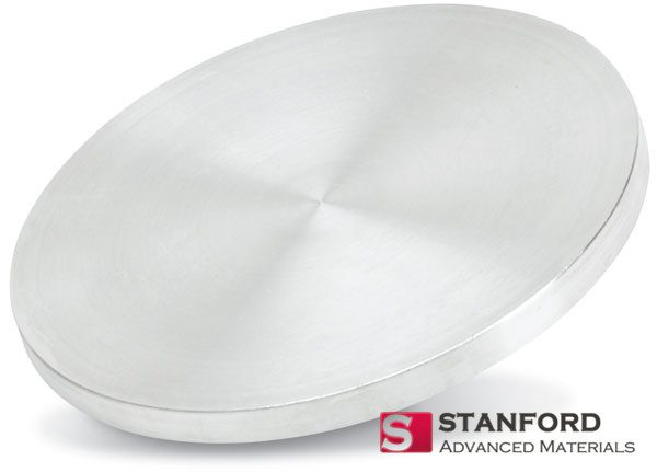
Tungsten sputter targets are a pivotal component in the physical vapor deposition (PVD) processes used across various high-tech industries, from semiconductor manufacturing to the production of thin films for photovoltaic cells. Here we’ll delve into what makes tungsten sputter targets unique and how they compare to other sputtering materials.
Definition and Characteristics
Tungsten, known for its high melting point and density, is an ideal material for sputter target applications that demand durability and high-temperature resistance. As a sputter target, tungsten offers several intrinsic properties:
- High Melting Point: At about 3422°C (6192°F), tungsten has the highest melting point of all metals in its pure form, which is crucial for sputtering processes that require high temperatures.
- Thermal Stability: Tungsten targets maintain structural integrity under extreme thermal stress, making them suitable for applications involving high power or long sputtering durations.
- Low Vapor Pressure: Its minimal vapor pressure at high temperatures ensures that the sputtering process remains consistent and stable, minimizing the loss of target material.
Comparison with Other Sputter Target Materials
Comparatively, tungsten sputter targets offer distinct advantages over other materials:
- Versus Molybdenum: While molybdenum is another popular sputter target material with excellent high-temperature properties, tungsten exceeds in durability and melting point, making it better suited for extremely high-temperature applications.
- Versus Aluminum: Aluminum targets are preferred for their higher electrical and thermal conductivity in applications requiring lower melting temperatures. However, for high-power applications that can lead to rapid degradation of the target material, tungsten’s robustness offers a longer lifespan.
- Versus Copper: Copper is favored in situations where thermal and electrical conductivity is paramount, such as in RF sputtering. However, tungsten’s superior resistance to thermal stress and slower erosion rate under similar conditions make it a reliable choice for wear-resistant coatings.
Applications of Tungsten Sputter Targets
Tungsten sputter targets find their applications in various industrial and technological fields due to their unique properties. Here, we explore some of the key applications and the role tungsten plays in each.
Semiconductor Manufacturing
In the semiconductor industry, tungsten sputter targets are used to deposit thin films necessary for the fabrication of integrated circuits. Tungsten is primarily used for the metallization process, where it serves as a conductive barrier layer and contact material due to its excellent electrical conductivity and resistance to electromigration.
Thin Film Coatings
Tungsten is extensively used in the production of thin film coatings for various applications:
- Wear-resistant coatings: Tools and components subject to high wear conditions, such as cutting tools and bearings, benefit from tungsten coatings that enhance durability and lifespan.
- Corrosion-resistant coatings: The chemical stability of tungsten makes it suitable for coatings that need to withstand harsh environments, protecting the base materials from degradation.
- Decorative coatings: Tungsten can also be used in thin films for ornamental purposes, providing a durable and aesthetically pleasing surface finish.
Photovoltaic Cells
In photovoltaic (solar) cell manufacturing, tungsten targets are used to create thin films that form part of the cell structure, improving the efficiency and performance of solar panels. Tungsten films can serve as barrier layers that protect sensitive materials within the solar cells from environmental damage while maintaining electrical conductivity.

Medical Devices
Tungsten sputtering targets are employed in the medical field to produce coatings for various devices. These coatings are particularly valued for their radiopacity, which enhances the visibility of medical implants and tools under X-ray imaging, aiding in precise placement and monitoring during medical procedures.
Challenges and Innovations in Tungsten Sputtering
Challenges in Tungsten Sputtering
Tungsten sputtering, while advantageous for various applications, faces several challenges that can impact the efficiency and quality of the sputtering process:
- High Melting Point: Tungsten’s high melting point (3422°C) requires sputtering systems to operate at elevated temperatures, demanding more robust equipment and higher energy inputs.
- Film Stress: Tungsten films can exhibit intrinsic stress which may lead to film cracking or peeling, particularly when deposited under certain conditions or at certain thicknesses. Managing these stresses is crucial for ensuring the durability and performance of the coatings.
- Target Bonding Issues: Due to their hardness and brittleness, tungsten targets are difficult to bond effectively to backing plates, which is a necessary step for efficient heat dissipation and mechanical stability during sputtering.
Innovations
To overcome these challenges, the industry has developed several innovative approaches:
- Advanced Target Bonding Techniques: New methods such as diffusion bonding and improved adhesive materials have enhanced the bonding of tungsten targets to backing plates, reducing delamination and extending target life.
- Stress Management Coatings: Innovations in layering and coating composition have been developed to manage and reduce intrinsic stresses in tungsten films. These include the use of buffer layers and the adjustment of deposition parameters to control film microstructure.
- Enhanced Cooling Systems: As sputtering technology advances, enhanced cooling systems are being integrated to manage the high temperatures involved in tungsten sputtering. These systems help maintain target integrity and improve the deposition rate.
These advancements are crucial for expanding the use of tungsten sputtering in industrial and technological applications. They not only address the immediate challenges but also open up new possibilities for the use of tungsten in areas where its properties are particularly beneficial.
Conclusion
The exploration of tungsten sputter targets across various applications and the ongoing innovations to overcome their inherent challenges highlight the dynamic nature of this field. Tungsten’s exceptional properties, such as high melting point, hardness, and thermal stability, make it an invaluable material in critical high-tech applications ranging from semiconductor manufacturing to medical devices.
As the demand for more sophisticated technologies grows, the role of tungsten sputter targets is set to expand further. Continued research and development are expected to enhance the efficiency and capabilities of tungsten sputtering processes, enabling wider adoption and new applications. This will not only improve the performance of existing technologies but also contribute to the development of innovative solutions that meet the evolving needs of industries worldwide.
For those in the industry, staying updated on the latest techniques and advancements in tungsten sputtering is essential. Companies like Stanford Advanced Materials (SAM) play a pivotal role in this sector by providing high-quality tungsten sputter targets and expert guidance to help businesses and researchers optimize their applications and achieve the best possible outcomes. As we look forward, the integration of tungsten into new technologies continues to hold a promising future, ensuring its place at the forefront of materials science and engineering innovations.
Click to Inquiry High Quality Tungsten Sputter Target


